


 Extract (6-MSITC) in Healthy Older Adults")
: An In-Depth Exploration into its Thermogenic Role and Social Significance")


A team of Rice University engineers has introduced the first neural implant that can be both programmed and charged remotely with a magnetic field.
Their breakthrough may make possible imbedded devices like a spinal cord-stimulating unit with a battery-powered magnetic transmitter on a wearable belt.
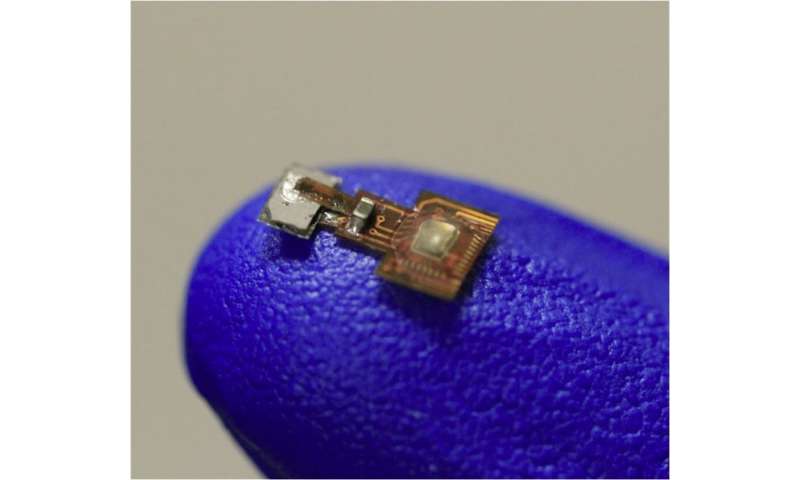
The integrated microsystem, called MagNI (for magnetoelectric neural implant), incorporates magnetoelectric transducers.
These allow the chip to harvest power from an alternating magnetic field outside the body.
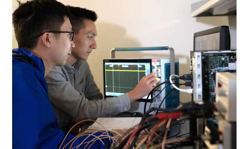
The system was developed by Kaiyuan Yang, an assistant professor of electrical and computer engineering; Jacob Robinson, an associate professor of electrical and computer engineering and bioengineering; and co-lead authors Zhanghao Yu, a graduate student, and graduate student Joshua Chen, all at Rice’s Brown School of Engineering.
Yang introduced the project at the International Solid-State Circuits Conference in San Francisco.
MagNI targets applications that require programmable, electrical stimulation of neurons, for instance to help patients with epilepsy or Parkinson’s disease.
“This is the first demonstration that you can use a magnetic field to power an implant and also to program the implant,” Yang said. “
By integrating magnetoelectric transducers with CMOS (complementary metal-oxide semiconductor) technologies, we provide a bioelectronic platform for many applications. CMOS is powerful, efficient and cheap for sensing and signal processing tasks.”
He said MagNI has clear advantages over current stimulation methods, including ultrasound, electromagnetic radiation, inductive coupling and optical technologies.
“People have been demonstrating neural stimulators on this scale, and even smaller,” Yang said. “The magnetoelectric effect we use has many benefits over mainstream methods for power and data transfer.”
He said tissues do not absorb magnetic fields as they do other types of signals, and will not heat tissues like electromagnetic and optical radiation or inductive coupling.
“Ultrasound doesn’t have the heating issue but the waves are reflected at interfaces between different mediums, like hair and skin or bones and other muscle.”
Because the magnetic field also transmits control signals, Yang said MagNI is also “calibration free and robust.”
“It doesn’t require any internal voltage or timing reference,” he said.
Components of the prototype device sit on a flexible polyimide substrate with only three components: a 2-by-4-millimeter magnetoelectric film that converts the magnetic field to an electric field, a CMOS chip and a capacitor to temporarily store energy.
The team successfully tested the chip’s long-term reliability by soaking it in a solution and testing in air and jellylike agar, which emulates the environment of tissues.
The researchers also validated the technology by exciting Hydra vulgaris, a tiny octopuslike creature studied by Robinson’s lab. By constraining hydra with the lab’s microfluidic devices, they were able to see fluorescent signals associated with contractions in the creatures triggered by contact with the chips. The team is currently performing in-vivo tests of the device on different models.
In the current generation of chips, energy and information flow only one way, but Yang said the team is working on two-way communication strategies to facilitate data collection from implants and enable more applications.
NEURAL recording implants offer great potential for studying the human brain in ways that were impossible just a few decades ago. This has inspired much research in the field, including three separate technologies: high-throughput complementary metal-oxide semiconductor (CMOS) array chips, high performance microelectrodes, and wireless power transmission (WPT) methods[1]. Some have spent research effort on CMOS sensor arrays in an effort to integrate a large number of high-performance amplifiers onto a single chip [2]–[7].
Others have focused on fabricating high quality electrodes designed specifically for probing into the brain [8]–[11]. Many have also powered these type of CMOS devices wirelessly [12]–[15]. Combining these technologies will enable studies of the brain to take place at a scale and density that was not before possible.
This study focuses on a device combining two of these technologies, a highly integrated CMOS neural recording chip, with wireless power transfer. CMOS amplifier arrays can be designed for any high throughput applications where a large number of parallel electrical measurements can be made. The CMOS device fabricated for this study is optimized for measuring neural signals while also integrating a high electrode count of 1024.
To achieve this high electrode count, while still allowing for a wireless data transmission, this CMOS device utilizes a pulse-based neural amplifier. Utilizing enhanced delta modulation (EDM) enables the high amplifier count by placing a modulator in each array element, making the outputs from each amplifier digital, rather than analog. This removes the requirement for one of the largest features traditionally found on CMOS amplifier arrays, the analog-to-digital converter (ADC). In fact, designing compact ADCs is a popular research topic [16]–[18].
In addition to removing the ADCs, placing a modulator in each array element has added benefits since digital signals are better suited to multiplexing and less susceptible to signal-related problems such as noise than analog signals. Additionally, the signals being digital immediately out of the amplifiers lends itself to high scalability, since additional multiplexing requires little circuitry and needs only a higher bandwidth communication channel.
A comparable analog system would require either faster (and therefore higher performance) ADCs, or additional ADCs to scale to higher array element counts. Both of these solutions would consume significant CMOS die area and power, effectively providing a limit for the number of amplifiers that can be integrated onto a single chip of the same size.
In this paper, the presented CMOS chip is mounted to a polyimide flexible printed circuit board (PCB) which contains additional electronics to facilitate a complete neural recording implant.
This flexible substrate enables the system’s wireless power transfer by using spiral traces as an inductive coil. It also holds a system-on-chip (SOC) that operates the CMOS chip and sends data wirelessly via Bluetooth low energy (BLE). The flexible nature of the thin polyimide-based substrate enables the implant to bend, allowing for the device to conform to the surface of the brain.
This paper discusses the design of the flexible neural implant and tests of its functionality. Section II describes the overall design of the device, describing the flexible substrate. In Section III, the circuitry and design of the coils for the wireless power transfer link are detailed. Section IV focuses on the neural recording amplifier design and the operation of the pulsed-based amplifier circuitry.
To demonstrate the functionality of the device, Section V presents results from the fabrication of the flexible implant and measurements of the wireless power transfer system, the neural amplifiers, the enhanced delta modulators, and the Bluetooth data transfer system.
FLEXIBLE NEURAL RECORDING IMPLANT
The flexible neural recording implant is a compact disk shaped implant that is wirelessly powered and thin enough to be implanted directly on the surface of the brain under the skull. An overview of the system is shown in Fig. 1.
The implant is small, only 15.4 mm in diameter by 2.0 mm at its thickest. The small size allows it to be placed on the brain under the skull. The flexible neural recording implant is fully wireless and does not require any wiring or battery to operate. Power is provided by an external coil, and data is transmitted wirelessly via BLE to a receiving device such as a laptop computer.

A. Flexible implant substrate
The core of the implant is the 15.4 mm diameter by 0.2 mm polyimide flexible substrate. Within this small space, the flexible implant contains electronics for the wireless power supply, the CMOS neural chip, and the SOC.
A block diagram for the flexible neural interface is shown in Fig. 2. The wireless power supply consists of a power coil that is implemented using spiral copper traces around the outer annulus of the substrate.
This coil is tuned to resonance via a parallel capacitor and fed into a full-wave bridge rectifier. The output of the rectifier is regulated using a 3.3 V regulator that powers the electronics in the neural interface. Signals are recorded via the EDM amplifier array integrated into the CMOS neural chip and sent to the SOC, a CC2640 (SimpleLink ultra-low power wireless MCU for Bluetooth low energy) by Texas Instruments. The SOC contains an ARM microcontroller that generates the required timing signals to operate the CMOS neural chip and processes and packages the data it receives to send via Bluetooth Low-energy. The SOC also contains a built-in BLE transceiver which is used to drive the external chip antenna through a balun.

INDUCTIVE WIRELESS POWER TRANSFER LINK
The fully wireless implantable device is powered by the use of a wireless power transfer link. This link consists of two sections, the external transmitter, and the wireless receiver coil on the flexible substrate.
The system is shown in Fig. 3. Briefly, the transmitter provides energy to the transmit coil which is inductively coupled to the receive coil on the neural interface, which resonates with this energy and is rectified and regulated to a stable voltage to power the electronics on the implant.

A. Inductive link coils
The most important components of the wireless power transfer link are the transmit and receive antennas. Previously, a method has been described which optimizes the coupling coefficient between two coils for wireless power transfer by carefully selecting their dimensions [14]. The method provides detailed data to choose the optimum dimensions based on two of the coil parameters presented in Fig. 3, z (the distance between the two coils) and RxOD (the receive coil’s outer diameter). For this neural interface, the coil separation z was set to 15mm as it is sufficiently large to fit the implant beneath the skull and skin. RxOD was also chosen to be 15 mm to be reasonably small and minimally invasive while still providing sufficient space for the electronics required for the implant’s operation. The other coil dimensions, RxID (the receive coil’s inner diameter), TxOD (the transmit coil’s outer diameter), and TxID (the transmit coil’s inner diameter) were chosen based on HFSS simulations.
B. Class E amplifier
For the most efficient operation of the wireless power link, the transmit coil is driven by a class E amplifier. The schematic for the class E amplifier is shown on the left side of Fig.3. The amplifier is based on a single power MOSFET that is driven by a logic-level square wave at the desired operating frequency f. LRF is an RF choke which is made sufficiently large for f. CTx is set so that a resonance occurs with LTx at f. The component values are chosen to maximize power delivery [19]. Power delivery to the transmit coil can be adjusted by varying Vsupply.
Provided by Rice University


