 Competitive Coexistence: Post-War Strategic Outlook")


 Extract (6-MSITC) in Healthy Older Adults")
: An In-Depth Exploration into its Thermogenic Role and Social Significance")


As we enter the wireless world of 5G, communications in the millimeter-wave band (i.e., from 30 to 300 GHz) will become increasingly important, particularly for high-speed wireless data-transfer applications.
The trouble is that at these small wavelengths, the on-circuit signal strength degrades rapidly, thus requiring the circuit to be highly integrated into the smallest possible footprint.
To best implement this, the high-frequency transistor technology needs to be compatible with the workhorse technology of digital electronics: complementary metal-oxide-semiconductors (CMOSs).
Recent studies have suggested that transistors made of aligned carbon nanotubes could lead to better performance in wireless devices than commonly used III-V semiconductors.
This is primarily due to their highly linear signal amplification and their better compatibility with CMOS circuits.
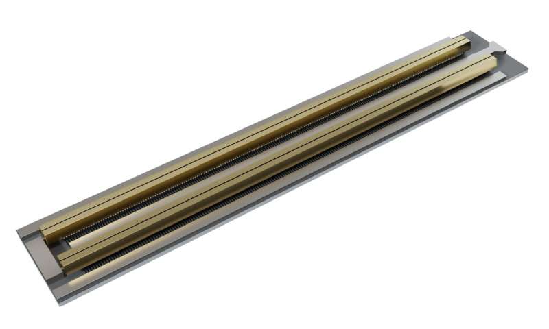
With this in mind, researchers at Carbonics Inc., a semiconductor electronics company based in Los Angeles, have recently developed a new type of transistor made of aligned carbon nanotubes.
This new transistor, presented in a paper published in Nature Electronics , operates at gigahertz frequencies and is easier to integrate with CMOS technology than most existing transistors.
“During my graduate studies, I worked with Prof. Peter Burke at UC Irvine (one of the original torch bearers for the technology) investigating radio-frequency applications for carbon nanotubes,” Christopher Rutherglen, one of the researchers who carried out the study, told TechXplore.
“After graduation, I continued the effort at a company called Aneeve LLC where the focus was on making high-frequency transistors using carbon nanotubes, using IP (intellectual property) licenses from Prof. Chongwu Zhou’s group at USC.”
Video animation showcasing the transistor. Credit: Rutherglen et al.
In 2014, Aneeve LLC, the company where Rutherglen was working, was re-incorporated as Carbonics Inc. after receiving substantial venture capital funding.
Since then, the company has been trying to develop and ultimately commercialize high-frequency carbon nanotube transistors.
The results, recently published in Nature Electronics, are a significant leap forward both for Carbonics Inc. and for the overall evolution of this particular type of transistor.
The key difference between the high-frequency transistors developed by Rutherglen and his colleagues and comparable incumbent technologies is that the former are made of thousands of aligned carbon nanotubes rather than higher-dimensional Si or III-V materials.
An important advantage of carbon nanotubes is that they are one-dimensional materials, and thus have superior transport characteristics.
“For example, as electrons are transported through any material, there is a tendency for them to scatter or collide along their path of travel, which ultimately reduces the speed of the overall device,” Rutherglen explained.
“In one-dimensional materials such as carbon nanotubes, electrons can travel much longer distances before scattering because there are fewer available states the electron can scatter into. Put simply: It cannot scatter up or down, right or left, because no such states exist in 1-D materials.”
A further advantage of carbon nanotubes in transistors is that they can be applied to a wide variety of substrates using a simple surface-coating method. This characteristic facilitates their integration with CMOS and other semiconductor technologies, as it makes them easier to combine with other materials.
“For nearly two decades, carbon nanotube-based high-frequency transistors have been touted as a game-changing technology,” Rutherglen said.
“However, the inflated expectations in those early days were not delivered upon, leaving many to subsequently discount the technology’s merits and move on. As reported in our paper, we have demonstrated for the first time that carbon nanotube high-frequency transistor technology can deliver incumbent-beating device performance in key metrics.”
The study carried out by Rutherglen and his colleagues opens up new possibilities for the development of transistors that are easier to integrate with CMOS circuits.
Their findings also suggest that the performance of transistors could be increased further by addressing some of the known challenges associated with developing this type of technology.
In the future, the results collected by this team of researchers could prompt change in the semiconductor industry, encouraging electronics manufacturers to reassess the design and structure of existing transistors. In order to take the aligned carbon nanotube transistors from a prototype stage to the mass-market, however, the technology will still need to receive investments of hundreds of millions of dollars.
“Our next step is to continue improving upon the results achieved and work with industry partners in furthering the technology along,” Rutherglen said. “We are currently engaged in licensing and technology transfer partnerships with industry participants.”
Capturing and isolating single atoms or molecules and controlling their quantum states to achieve the desired function is undoubtedly a fantastic milestone for toolmaking and information processing, the two pillars of human endeavors.
Stimulated by successful demonstrations, such as trapping a single atom or imaging single atomic sites and bonds within a molecule, there have been visions to reach beyond nanotechnology for continuing at thousand times smaller into the pico-technology [1], and at a million times smaller into the femto-technology [2], the realm of neutrons, protons, electrons, and other nuclear particles.
Amazingly, pico- and femto-technologies are already being contemplated for addressing technology bottlenecks, such as a better electronic on-off switching speed to improve communication bandwidths beyond ~50 GHz [3].
In the earlier stages of nanotechnology, in “Technical boundless optimism”, D. Jones, reviewing “Nano! Remaking the World Atom by Atom”, raised certain skepticism with respect to the promises and potentials of nanotechnology [4].
However, demonstrations, such as resolving the atoms that make up the benzene rings within a molecule (pentacene) adsorbed on a copper or a sodium chloride surface [5], uphold the noted optimism.
Resolving the atomic structure of graphite, monitoring the formation of fullerene C60 molecules [6], and discerning the various carbon-carbon bonds within the molecules [7] are other examples of boundless success.
In “Bonding more atoms together for a single molecule computer”, C. Joachim discussed how the future of computing would depart from solid-state integrated electronics and enter the realm of molecular transistors [8].
Such claims are already being supported by works on single molecules, for example, controlling cis-trans transition in Azobenzene molecule, leading to the molecules being “switched” with spatial selectivity, has been demonstrated [9].
Taming individual atoms towards quantum computing, atom-by-atom assemblers to arrange several trapped neutral atoms in one-dimension [10], in arbitrary two-dimensional patterns [11], and in three-dimensional arrays [12] with controllable single atom capability, have been demonstrated.
To scale up the “fabrication” of such atomic and molecular switches, novel concepts are being reported, including the demonstration of monolayer surface patterning at 3.5 nm on a gold surface via self-assembly, offering a potential path to large-area patterning [13].
Assessing the joint impact of nanosystems that function as sensors, actuators, processors, memory, and communication links is nontrivial.
For example, the importance of electronic computers in investigations of molecular quantum mechanics was recognized as early as 1956 [14]. However, the notion of molecules themselves being used as computers, or quantum effects being employed to compute and communicate, have only emerged recently.
Astonishingly, DNA computing [15], molecular machines [16], biological microprocessors [17], bio-electronic computers [18], etc. have been already reported, albeit largely exploratory.
Nevertheless, aided by nanosystems, information is being created at rapidly increasing rates. Reciprocally, the explosive growth of data [19] and its profitable global market [20] is rapidly advancing the exploration and discovery of new nanosystems that can statically and dynamically accommodate information [21].
The generation and fate of information and its fascinating dynamic relationship with information technological devices warrant scrutiny [22,23,24,25,26,27]. Morphing into a countless number of sensors [28,29,30], data collectors are generating mindboggling amounts of data [31], soon to reach ~1021 bytes (or zettabytes, ZB) [32]. A 2012 industrial study reported an estimated 1 ZB of data generated worldwide with a predicted 40 ZB by the year 2020 [33].
In year 2011, Hilbert and López, estimating the world’s technological capacity to store, communicate, and compute information, concluded that in the year 2007, the world had stored ~0.29 ZB (compressed bytes), communicated ~2 ZB, and carried out 6.4 exaflops (=6.4 × 10¹⁸ flops or floating-point operations/s) [19].
For comparison, Hilbert and López noted that the exaflop rate roughly equals the maximum number of nerve impulses/s executed by one human brain, and the ZB stored data is approaching the roughly 100 ZB stored in the DNA of a human adult [19].
With computing operation rates at the exaflop in the horizon [34], the high-performance computing (HPC) has to possess the capability to handle exabyte (~1018 bytes) massive quantities of data in addition to improved flops. The processing, communication, and storage of the large volumes of data by transistor circuits, interconnects, and networks, invented to make use of the digitally represented information, are pervasive.
However, these operations are growing increasingly challenging due to data traffic, memory, and computing capacities. To combat the challenges associated with the need to transfer and communicate large amounts of data generated in one location to an HPC data center in a different location, the concept of edge computing (EC) [35] is being intensively investigated [36,37,38,39].
The intent of this article was a survey of the general state of the EC and the pertinent nanoscience subfields, including nanophotonics [40,41,42,43,44,45] and nanomaterial-based components [46,47]. Noting the cross-disciplinary nature of the solutions needed to overcome existing challenges in EC, we discussed how the relevant research areas and technologies could be mutually beneficial towards serving the needs of the internet of things (IoT) and HPC in the exascale regime.
A growing number of exploratory work of potential for the next generation computing is being reported, e.g., creating and controlling Majorana quasiparticles for use in quantum computing [48], or use of metamaterials in optical computing of integral equations [49].
However, while several exciting venues have opened up towards achieving stable information carriers for quantum computing or biologically inspired massive processing, we here emphasize developments that have been recognized to be closer to scalable implementation.
Skyrmions, for example, are spatially highly localized (~nm) excitations or quasiparticles in a magnetic material. They exhibit a level of stability, mobility, and localization that render them highly suitable for information encoding. These magnetic spin configurations are protected by the specific topology of the underlying material domain (e.g., a ferromagnet-heavy metal bilayer [50]).
Thus, they can be transported and manipulated to convey information, leading to the notion of Skyrmionics, which has been proposed for stochastic or probabilistic computing [51].
However, probabilistic computing (compared to binary-encoded computation) is itself under active exploration to potentially provide an alternative computing platform for embedded systems at lower area and power, and better error resilience, and high computational density, all of which are ideal attributes for constrained environments, such as EC devices (sensor nodes and mobile devices) [51,52,53].
Skyrmionics, however, is not considered sufficiently developed to compete with existing silicon electronics. Figure 1 displays some elementary statistics related to EC, emphasizing the recent rapid growth and the diversity of EC research profile. We noted that the key discussion of the article, that is, the use of nanotechnology in the development of EC, pertains more generally to the next generation computing systems rather than specifically to EC.

Article statistics showing the histogram of edge computing over publication years, a compilation from [54]. Inset: distribution by discipline [54]. Notable are the intensified research, the multidisciplinary character of the field, and the largest contributing disciplines. The number of other contributing disciplines (not shown) is also increasing rapidly.
Edge Computing
Edge computing may be regarded as a product of the evolution of electronics and communication. In “How we created edge computing” [35], M. Satyanarayanan discussed how the realization of the limitations of cloud-based processing led to the proposal of the concept of EC via the introduction of cloudlets [55,56,57]. While sharing similarities, clear distinctions exist between cloud, cloudlet, fog, and edge [37,38,39]. Satyanarayanan et al. subsequently showed that reductions of 51% and 42% in latency and power use, respectively, could be achieved in a mobile device when using cloudlets (in this case, a virtual machine on Dell Optiplex 9010) instead of the cloud (Amazon EC2).
In “Working on the edge”, further definition of EC was provided by V. Bahl, who also discussed the future of EC, and how it would help the cloudification of the telecom network and become an integral component of it. Interestingly, Bahl further characterized the EC as a “marriage” between the telecom and the IT industries [58]. While the definition of EC may be subject to slight variation and remains largely broad, for the sake of our presentation, we showed the common ingredients in Figure 2.

Some basic elements of a device in the edge computing paradigm. The edge device does not necessarily require a connection with a centralized cloud. Many challenges lie ahead regarding energy efficiency, data quality and reliability, data and device security, computing performance level, etc., stimulating exploration for novel nanosystems and processor architectures, rapid communication, and related components.
Examining the rapidly growing number of investigations reported (see Figure 1), the following recurring definition takes the center stage: EC is an emerging data processing paradigm toward countering the current and projected bottlenecks of cloud-based computing. Thus, EC strives to complement the cloud. An EC device processes data on local computing and communication infrastructure and only, if necessary, prepares data and establishes a communication link to a data center or other EC devices.
Therefore, EC is envisioned to overcome both latency and memory bottlenecks of the current centralized cloud-based paradigm. However, despite recent related surveys [37,38,39], exactly how an EC device should be defined has not been rigidly formulated due to the infancy of the EC field and the high degree of diversity of IoT. Nevertheless, we may recognize that to constitute an EC device, innovations in both hardware and software are necessary to meet the growing speed and memory requirements.
EC devices take on the task of carrying out preliminary data processing instead of transmitting raw data to data centers for processing. Aiding the cloud by greatly reducing the upload bandwidth and computation complexity, the EC nodes are envisioned to perform tasks, such as real-time signal and image processing, combinatorial optimization, agent-based modeling, big data analysis, etc. Such tasks are performed to provide secured services, effective control, and seamless decision-making while achieving energy efficiency.
Therefore, HPC is essential to EC networks [59]. In recognition of the importance of the EC field, in, a recent, editorial “Take it to the edge” [60], it was named the 2019 technology of the year.
A central objective of cloud, fog, mist [61], and recently EC, has been to achieve enhanced performance locally using a non-centralized distribution of computer memory and computing power (see). The advantage of offloading computational tasks to fog or cloud servers is a time reduction for task processing. Thus, physically, servers are deployed at the near edge or the extreme edge of the network (closer proximity to the data sources) instead of the data centers [62].
Specifically, EC is addressing the challenges facing the computing of data for which speed and scale are not only ideal but necessary. Despite the power of the cloud computing and storage solutions (e.g., platforms, such as Amazon elastic compute cloud [63] and Google cloud platform [64]), the increasing number, type, and spatial distribution of devices, generating extremely large amounts and types of data, require continuous innovation. Therefore, the infrastructure is evolving from its core, i.e., the data centers to its edges. The diversity in the IoT applications implies that data processing may require different levels of intelligence, efficiency, and security.
As the technologies could generate predictions about personal behaviors and private lives, measures must be considered to guard against the associated pervasive analytics.
An important issue of EC is dealing with data protection, as discussed in “Data protection in the age of big data” [65]. Recently, in “Multi-tier computing networks for intelligent IoT”, as depicted in Figure 3, Y. Yang defined the roles of cloud, fog, and edge computing technologies; delineated their hierarchies; and described how integration among them might be necessary for optimum IoT services [66].

Multi-tier computing networks. The integration of various technologies to achieve intelligent applications and services.
Increasingly advanced sensors with sophisticated data acquisition (software and hardware) are being employed globally. In sensing, a simple use case is that of a single sensor or a network of complex integrated sensors [67] reporting a single or arrays of parameters, e.g., extracted from a terrestrial or an extraterrestrial environment. As an example, consider a sensor for the detection of environmental methane, mercury, fungi, or bacteria.
As depicted in Figure 4, a raw signal is produced by the sensor, which within some calibration is representative of or proportional to the presence of the sought chemical or biological species. To create useful information and decision-making, the raw signal is either (I) communicated directly to the cloud via a network for processing and storage, or (II) is first somewhat processed locally and then communicated to the cloud.

Example of a current paradigm based on cloud computing. Sensors generate raw signals, which are submitted to the cloud directly (route II) or are acquired and observed and then either communicated to the cloud or are evaluated and submitted to the cloud.
Within the IoT, the number of sensors is exploding, and thus feeding or uploading such raw or insufficiently processed varying sized signals is readily seen to lead to bandwidth, latency, and storage problems [68]. For example, smart cities [69], homes, and cars will generate a heretofore unimaginable amount of data and communication loads. EC is envisioned to alleviate such predicted/expected problems.
By incorporating a local high-performance processor with built-in artificial intelligence (AI), local decision-making can be carried out and only if necessary, communicated with the cloud. This is depicted in Figure 5, where the raw data is locally processed in an embedded processor with sufficiently provided AI (e.g., Fuzzy logic, Bayesian network) to generate high-level information and confident decisions. The output information, instead of the raw data, may then be communicated to the cloud for further processing (HPC, storage, etc.).

A simplified edge computing approach. A sensor generates raw data, which is locally processed and evaluated. If the outcome meets certain criteria, the data is then communicated to the cloud for further processing/computing and storage.
Distributed sensing, such as used in the oil and gas industry, is expected to be a major beneficiary of EC. For instance, spatially distributed, fiber optic sensors, capitalizing on Brillouin and Raman scattering [70], interact and detect pressure, vibrations, gas species (leaks and contamination), temperature, and other harsh-environment parameters for fossil energy research [71]. Due to its distributed nature, EC encompasses many of the same aspects of signals, processing, computing, and data storage. As a result, within the IoT, including IIoT (industrial IoT [72]) and IoMT (internet of medical things [73,74]), the EC devices are extremely diverse, and the volume of data they are generating and processing is rapidly increasing.
Data formats include time and frequency space signals, complex images, sound and voice, and a plethora of protected health [74,75,76], personal, and sensitive data. Due to the variety of EC devices, data types, and algorithms [77], many AI-based or smart offloading and transmission strategies are being proposed, such as employing machine and deep learning methods [75,78], or mimicking human brain networks [79].
Similarly, knowledge-sharing strategies to take advantage of self-taught knowledge between EC devices, such as pertaining to home IoT, have been considered [80]. Undoubtedly, EC-specialized or related optimization problems formulation and solution will be valuable [72,81,82,83], as discussed in the case of optimization consideration for platooning for automatic driving [84], evolutionary game theoretical proposals for mobile devices and security [85,86], better estimation of interference in EC devices [87], cost-effective placement of EC servers [88], computational power allocation for blockchains [89], and incorporation of computer vision [90].
While security strategies are being developed [61,91,92], the emerging era of EC offers tremendous opportunities for research and development in nanosystems, such as optical sensors, optical communication, and photonic processors [40,41,42,44,93,94], all of which are to be seamlessly integrated in one or more part of the secure network, from the edge to the core.
The increased computational loads on end EC-based devices, in conjunction with IoT operating system, is to consider balanced process management for the interplay between the processing and communication tasks [95] or resource and energy consumption [96]. In an empirical study using IoT sensor devices, tests were carried out with different levels of computational load and various priority schemes to show that an increased load results in cross-effects between the processing and communication tasks, significantly affecting their performance [95].
The decentralized decision-making of the EC paradigm toward generating accurate data must be energy efficient. For example, the continuous readings to provide high-resolution location can be energy inefficient in mobile devices prompting proposals to develop on-device cognitive-inspired control for power-aware human mobility analysis in IoT devices [97].
In addition to energy efficiency, the emerging EC, aiming to provide faster IoT operation and mobile devices, seeks to conserve and optimize memory, cache, server placement, size, weight, etc., calling for new studies and proposals. Recently, to realize a potentially scalable and intelligent caching scheme that aims to reduce cache redundancy, a progressive popularity-aware caching scheme was proposed [98].
To avoid wasting cache space when the content is not popular enough, the proposed method first caches initial “chunks” of the content at the edge node and then progressively continues caching subsequent chunks at upstream according to the content popularity and each content node position [98]. Also, the cost-effective placement of edge servers has been proposed for metropolitan area network [88].
The universality of EC applications and the accumulative impact they will impart can be readily appreciated from the long list of applications that are rapidly growing into various hierarchies of service. For example, for more reliable service, solar cells/panels and related devices need to become smart with AI for IoT in an EC domain.
Spectral variation, combined with an array of environmental sensors to monitor, pressure, temperature, humidity, wind speed, cloud movements, etc., can be utilized to optimize the performance of solar cells, leading to potentially significant economic benefits. Similarly, traffic lights augmented with hyperspectral imaging and chem-bio sensors can be made locally smart when combined with weather sensors and the unique local population and infrastructure signatures.
More concrete EC applications include scalable framework for early fire detection [99], disaster management services [100], accelerometers for structural health monitoring [101], micro-seismic monitoring platform for hydraulic fracture [102], a framework for searchable personal health records [75,76,103], smart health monitoring [76,104] and healthcare framework [105], improved multimedia traffic [106], a field-programmable gate array (FPGA)-based system for cyber-physical systems [107] and for space applications [108], biomedical wearables for IoMT [73,76,109], air pollution monitoring systems [110], precision agriculture [111,112], diabetes [74] and ECG [109] devices, and marine sensor networks [113].
Acute needs of edge devices are readily identified within the customs and border protection (CBP), where agents controlling illicit drugs and contraband can immediately make decisions instead of communicating with other data centers. With the opioid crisis, the number of sensors will inevitably increase, and EC devices with sufficient computing power and rapid communication rate can provide critical decision-making.
Since the EC devices, such as IoT sensor nodes, will be ubiquitous, embedded computing paradigms for EC devices will have to use energy-efficient microprocessors to process the data. Furthermore, supplying real-time on-demand energy for EC devices will have to be investigated, in particular, since the energy consumption rate changes dynamically at different nodes prompting new charging scheduling schemes [114].
For chemical and biological sensors, real-time data acquisition, rapid processing, and computing are necessary. If the sensor output can be processed locally, instead of being sent to a different location, better mitigation and remediation can be achieved. A closely related EC-use case is the need for intelligent surveillance cameras. With the tremendous need for chem-bio standoff detection, the ability to collect molecular spectral data in addition to visual information would revolutionize the surveillance technologies. Aided with AI, EC surveillance cameras will be capable of processing the local streaming and only communicate specific detection results rather than continuous submission of the data. Upon reception, the cloud could then send the EC device new instructions, including programming to different functionalities.
Increasingly more complex services are expected to be provided by the continuously improving energy efficiency of system-on-chip (SoC), furnishing sensors and devices (edge, mist, fog, and IoT end devices) with significant computing power. This allows a self-contained module in which edge sensors and actuators generate data that can be processed on-site. In addition to software, SoCs, containing components, such as processors, graphics processing unit GPU), network-on-chip (NoC) [115], and memory and data storage, essentially function as a server. Attractive/desired attributes of SoCs include their SWaP (size, weight, and power).
Given the staggering number of future EC devices, it may be prudent to treat certain dynamic aspects of the EC within the realm of coupled oscillator systems and self-similar geometries, as graphically depicted in Figure 6. One may then ask the question of specific distributions of EC devices corresponding to holistic and emergent information phenomena.

Envisioning a potential variation of the interconnectivity of edge sensors. The nested growth of edge devices may form a system of a coupled dynamical system with fractal self-similarity. The sensor output S can be processed to H and communicated as N with a final output of f for node i located at Ri relative to data center Os.
Although there is an increasing number of EC-related optimization work being reported, obtaining quantitative data on the figure of merit of EC is less prevalent in the current state of affairs. Such quantitative data would provide energy consumption merits or other advantages of EC. For example, in a fog versus cloud computing experiment, in which 25% of the applications needed real-time services, around 40% reduction in energy expenditure was reported for the fog [37].
Similar reports are emerging, where also EC advantages are being specifically compared to cloud computing.
For example, an edge micro-seismic monitoring system was shown to perform at higher efficiency with less transmitted data when compared to a method lacking edge capability [102].
EC-specific quantitative metrics is currently highly needed. Unlike cloud computing simulation frameworks (including the cloud-based EdgeCloudSim simulator [116]), simulators that could be specifically used for modeling the design and behavior of an EC device are not quite available yet [36].
Given the very broad scope of computing, our review encompassed a brief account on the emerging nanomaterials and nanosystems of potential use in computing. Discussions pertaining to the many types of processors: central processing unit (CPU), GPU, FPGA, etc., architectures (multi-core, heterogeneous core processors, neuromorphic, etc.), and related hardware and software are presented marginally [117,118,119].
More information: Christopher Rutherglen et al. Wafer-scalable, aligned carbon nanotube transistors operating at frequencies of over 100 GHz, Nature Electronics (2019). DOI: 10.1038/s41928-019-0326-y
Journal information:Nature Electronics


