


 Extract (6-MSITC) in Healthy Older Adults")
: An In-Depth Exploration into its Thermogenic Role and Social Significance")


Perovskite nanocrystals hold promise for improving a wide variety of optoelectronic devices—from lasers to light emitting diodes (LEDs) – but problems with their durability still limit the material’s broad commercial use.
Researchers at the Georgia Institute of Technology have demonstrated a novel approach aimed at addressing the material’s durability problem: encasing the perovskite inside a double-layer protection system made from plastic and silica.
In a study published Nov. 29 in the journal Science Advances, the research team describes a multistep process to produce encased perovskite nanocrystals that exhibit strong resistance to degradation in moist environments.
“Perovskite nanocrystals are highly susceptible to degradation, particularly when they come into contact with water,” said Zhiqun Lin, a professor in the Georgia Tech School of Materials Science and Engineering.
“This dual-shelled system offers two layers of protection while allowing each nanocrystal to remain a distinct and separate unit, achieving the maximum amount of surface area and other physical characteristics of the perovskite needed for optimizing optoelectronic applications.”
The term perovskite refers to the crystal structure of the material, which is generally composed of three parts: two cations of different sizes and an anion in between.
For decades, researchers have tested substituting various chemicals into the structure to achieve unique characteristics.
In particular, perovskites containing halide compounds such as bromide and iodine can act as light absorbers and emitters.
For this study, which was supported by the Air Force Office of Scientific Research, the National Science Foundation, the Defense Threat Reduction Agency, and the Department of Energy, Lin’s group worked with one of the most common halide configurations, which is formed from methylammonium, lead, and bromide.
Their process involves first forming star-shaped plastic molecules that could serve as “nanoreactors” by growing 21 polymer arms on a simple sugar molecule. Then, once precursor chemicals for the silica and perovskite nanocrystals are loaded onto the plastic molecule, several stages of chemical reactions produce the final system.
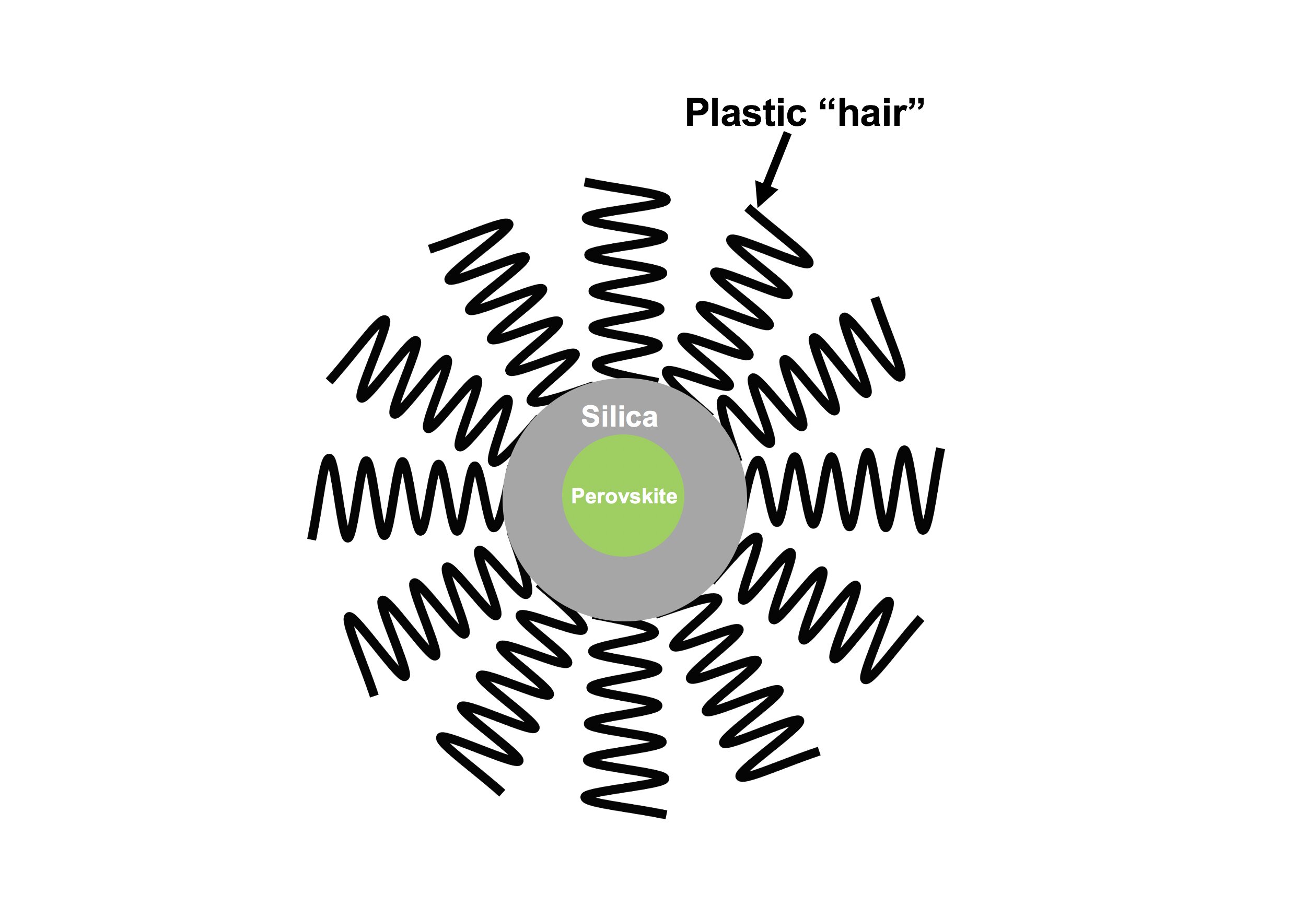
After the star-shaped plastic has played its role as a nanoreactor, the star-shaped components remain permanently attached, almost like hair, to the silica, which encases the perovskite.
The hairs then serve as the first layer of protection, repelling water and preventing the nanocrystals from clumping together.
The subsequent layer of silica adds further protection should any water get past the water-repelling plastic hair.
“Synthesis and applications of perovskite nanocrystals have been a rapidly evolving research field over the past five years,” said Yanjie He, a coauthor of the paper and former graduate student at Georgia Tech.
“Our strategy, based on a judiciously designed star-shaped plastic as a nanoreactor, enables unprecedented control in the crafting of high-quality perovskite nanocrystals with complex architecture, which is inaccessible in conventional approaches.”
To test the material, the researchers coated glass substrates with a thin film of the encapsulated perovskites and conducted several stress tests, including immersing the entire sample in deionized water.
By shining ultraviolet light upon the sample, they found that the photoluminescent properties of the perovskites never diminished during a 30-minute test.
For comparison, the researchers also immersed unencapsulated perovskites in water and watched as their photoluminescence vanished in a matter of seconds.

Lin said the new method unlocks the possibility of tuning the surface characteristics of the dual-shelled nanocrystal to enhance its performance in a greater range of applications. The process of fabricating the new perovskite nanocrystals from the star-shaped plastic was also unique in that it employed low-boiling point solvents with low toxicity.
Future research may center on developing different perovskite nanocrystal systems, including all-inorganic perovskites, double perovskites, and doped perovskites.
“We envision that this type of perovskite nanocrystal will prove very useful for creating durable optoelectronic devices for bioimaging, biosensors, photonic sensors, and radiation detection, as well as next generation LEDs, lasers, and scintillators,” Lin said.
“This is because these hairy perovskite nanocrystals carry unique advantages, including high defect tolerance, narrower emission bands, and high scintillation efficiency.”
In the search of high-efficiency, low-cost solar cells, a multitude of new materials and architectures are currently being explored. Over the past decade, organometal halide perovskites (OHPs) have emerged as a highly promising photovoltaic material and have been demonstrated as the active layer in perovskite solar cells (PSCs) with efficiencies over 25% for laboratory-based devices (~0.1 cm2) [1] and around 10–15% in modules [2] and are recently being employed in high-efficiency tandem devices [3].
The performance of PSCs has seen a meteoric rise over the past decade and they are already comparable with or superior to well-established photovoltaic technologies [1]. OHPs are attractive particularly due to their ease of processing [4], large absorption coefficients [5], long carrier diffusion lengths [6], low exciton binding energies [7], and low non-radiative recombination rates [8].
These properties also make OHPs an attractive material for various other optoelectronic devices, such as light emitting diodes [9], lasers [10,11], and photodetectors [12].
OHPs have a perovskite crystal structure with the general stoichiometry ABX3 as shown in Figure 1. The A-site is occupied by a monovalent cation e.g., methylammonium (MA, CH3NH3+), formamidinium (FA, CH3(NH2)2+), Cs+ etc. The B-site is usually occupied by a Pb2+ divalent metal cation and can be substituted by a similarly-sized divalent cation such as Sn2+. The X-site is usually occupied by a halide anion e.g., I−, Cl−, Br−. OHPs with mixed cations and/or anions are now the standard for high efficiency cells, particularly due to improved structural stability [13,14,15].
Their high compositional tunability, whereby the bandgap can be easily modified through ion substitution [16] and low-cost facile deposition procedures [17] makes OHPs excellent candidates for tandem solar cells, where two materials of different bandgaps are employed in conjunction to absorb different parts of the solar spectrum.
OHPs can be employed either as the top cell in a tandem device (with e.g., silicon, cadmium telluride, copper indium gallium diselenide etc. bottom cell) or in a stacked perovskite–perovskite tandem device. The successful fabrication of tandem cells with OHPs has the potential to achieve efficiencies in excess of 40% [3].

Cubic perovskite unit cell.
While OHPs have demonstrated remarkable efficiencies in laboratory solar cells, there remains significant challenges regarding long-term suitability and feasibility of commercialization [18]. OHPs are extremely susceptible to moisture-induced degradation, and therefore devices must be fabricated in controlled nitrogen atmospheres to avoid trapped moisture in the active layer. Furthermore, devices must be sufficiently encapsulated to prevent external moisture ingress, and the fragility of OHPs along with weak inter-layer adhesion may demand rigid glass substrates to avoid delamination or fractures in the OHP.
Even so, heat and light cycling can still induce degradation in encapsulated devices due to thermal mismatch [19]. The use of encapsulants, which can be expensive, along with rigid glass supports, makes OHPs less attractive due to increased costs [3]. It is therefore highly desirable to develop perovskite materials which are stable and tolerant to moisture and other environmental stresses.
Forming nanostructured OHPs (also referred to as low-dimensional OHPs) can be a potential route towards increasing the stability. So far, various types of low-dimensional OHPs have been demonstrated in solar cells, and typically show far superior stability to bulk OHPs [20,21,22]. This is achieved particularly due to higher formation energies of the low-dimensional perovskite structure and the possibility of encapsulating low-dimensional OHPs in long-chain polymers, essentially providing a protective barrier to moisture [22].
However, carrier transport tends to be restricted in nanostructured perovskites due to the presence of potential barriers within the nanostructured OHP, while quantum confinement also tends to widen the bandgap towards values typically in excess of 2 eV. This therefore comes at a cost to the performance, with the best nanostructured OHPs performing between 10–18% [20,21,22,23,24].
Considering the recent advances in nanostructured perovskites, here we will provide an insight into the important developments and progress in photovoltaics. First, an introduction to the use of bulk OHPs in solar cells will be provided while discussing the challenges and issues facing these materials in order to provide a context for the recent direction towards nanostructured perovskites.
This review will then provide a perspective into nanostructured perovskite solar cells as a possible route towards overcoming the issues pertaining to bulk OHPs.
Furthermore, hybrid devices formed with OHPs and nanocrystals (NCs) will be discussed, along with high-stability metal oxide perovskite nanocrystals. We hope this will provide the reader with a basis for understanding the current status of PSCs and the potential opportunities of stable, low-dimensional perovskites.
Overview of Bulk Perovskite Solar Cells
PSCs were initially inspired by the dye-sensitized solar cell (DSSC), where simply replacing the dye in a DSSC with an OHP immediately yielded efficiencies of ~3% [25]. The OHPs used were either MAPbI3 or MAPbBr3, where MA is the small organic cation methylammonium (CH3NH3+). Since the liquid electrolyte, which is used in DSSCs as a redox mediator, dissolved the OHP, these devices had very short lifetimes on the order of seconds.
The rapid dissolution of the OHP was overcome by replacing the liquid electrolyte with a polymer which did not dissolve the OHP. Subsequently, devices were reported using the polymer spiro-MeOTAD for hole transport, quickly achieving efficiencies of ~10% with improved device lifetime [26,27].
It was demonstrated that electron and hole transport occurs in the OHP, indicating that free-carriers are generated in the OHP with long diffusion lengths and lifetimes, contrary to suspicion that photocarriers would be excitonic as for organic solar cells, and therefore the sensitized architecture was in fact not necessary [26].
The main PSC device architectures are shown in Figure 2. The OHP is sandwiched between two selective contacts, an electron transport layer (ETL) such as TiO2, and a hole transport layer (HTL) such as spiro-OMeTAD. Metallic contacts are formed on either side of the transport layers: a window contact is formed using a transparent conducting oxide (TCO) such as indium-doped tin oxide (ITO), and a back contact is formed using either gold, silver, aluminum etc. The first architecture employed in the research timeline was the sensitized architecture using a thick mesoporous layer of TiO2 (Figure 2a).
This was quickly replaced with bi-layer devices, where the mesoporous-TiO2 was reduced in thickness and a thicker OHP layer was deposited to allow for greater absorption of light and longer crystalline order with larger grain sizes (Figure 2b). A planar device architecture can also be used, with either n-i-p configuration (Figure 2c) or p-i-n configuration (Figure 2d).
The planar device eliminates the necessity for the mesoporous TiO2 layer, further reducing fabrication costs and complexity. Planar devices show greater potential for low-cost roll-to-roll printing of PSCs at low temperatures due to the elimination of mesoporous-TiO2 which must typically be annealed at high temperatures during device fabrication (~500 °C) for high-efficiency PCSs, and is therefore unattractive for large-scale production while also eliminating the possibility of fabricating devices on flexible plastic substrates. Furthermore, the high-temperature annealing of TiO2 is not suitable for the fabrication of tandem devices with silicon or perovskite bottom cells since such high-temperature annealing process will damage the silicon bottom cell [3].
Planar devices using an SnO2 electron transport layer can be fabricated via low-temperature methods and demonstrate superior stability to mesoporous-TiO2 devices, however the best efficiency of 21.6% is somewhat lower than mesoporous-TiO2 devices (25.2%) [1,28].
Since PSCs employing mesoporous-TiO2 transport layers have shown greater efficiencies than planar devices thus far [29], ideally low-temperature fabrication techniques should be developed for mesoporous-TiO2 transport layers to enable their incorporation into tandem devices.

Various device architectures for organometal trihalide perovskite solar cells. (a) Mesoporous sensitized, (b) bi-layer, (c) n-i-p planar and (d) p-i-n planar. ETL, HTL, and TCO stand for electron transport layer, hole transport layer, and transparent conducting oxide, respectively.
Stability of Perovskite Solar Cells
While exceptional efficiencies have been demonstrated with Pb-based perovskites [13,14,15], significant challenges exist such as poor stability, toxicity, and rate-dependent current-voltage hysteresis. Stability is an important consideration when assessing commercialization viability of new materials given that silicon solar cells can easily operate for >25 years, even when exposed to a broad range of temperatures and intense solar irradiance.
OHPs tend to degrade rapidly in open air conditions and must be fabricated in controlled atmospheres to avoid moisture contamination. The rapid degradation of MAPbI3 in open-air conditions is shown in Figure 3, where the majority of the MAPbI3 layer degraded to PbI2 within 13 days [30]. Although the exact mechanism of degradation remains unclear; it is generally understood that an intermediate phase is first formed via hydration of the OHP [31,32].
Considering the decomposition of MAPbI3, the hydration of MAPbI3 leads to its conversion to MA4PbI6·2H2O and PbI2, followed by phase separation and the subsequent loss of MA, with the final products being CH3NH3I, PbI2, and H2O [31].
The degradation has been shown first to occur at the grain boundaries and is assisted by the presence of trapped charges which usually exist at defect sites, surfaces, and grain boundaries [33].
Ions can easily migrate within OHPs, causing charge accumulation, phase segregation, lattice distortions, and strain in the perovskite structure [34,35,36,37,38]. The degradation of OHPs is enhanced under illumination, and degradation can be accelerated even under moderate temperatures of ~60 °C [39,40].
Furthermore, I2, which is generated within the OHP due to exposure to moisture, can easily migrate and leads to the self-sustaining and irreversible degradation of the OHP [41].
The degradation of OHPs leads to the release of the gaseous products CH3NH2, HX, CH3X, and NH3 (where X is a halide), and the release of these gases can be observed at temperatures below 70 °C [42].

Degradation of MAPbI3. (a) Photographs of MAPbI3 degradation and (b) corresponding X-ray diffraction (XRD) spectra of the same samples after 1, 13, and 26 days stored in ambient conditions. The starred peaks in the XRD spectra correspond to PbI2. Reproduced from ref. [30], with permission from John Wiley and Sons, 2016.
Due to the high susceptibility of OHPs to degrade when exposed to moisture, it is therefore necessary to carefully control the atmosphere during fabrication. Entire device encapsulation is necessary to prevent exposure to moisture and mechanical fractures. For encapsulated devices, the formation of bubbles has been observed in the encapsulant layer due to the release of gaseous species.
Encapsulation prevents gaseous products from escaping, creating a thermodynamically enclosed system which is expected to reduce the rate of degradation [42].
Encapsulation is therefore essential for several reasons: to prevent the ingress of moisture; to prevent the release of gases; and to prevent the release of toxic materials to the environment. However, due to the thermal expansion coefficient mismatch between the various layers, including the encapsulant, temperature cycling of the PSC (i.e., day and night temperature variations) can lead to significant delamination and device failure. Careful selection of the encapsulant and various device layers is therefore necessary to minimize delamination caused by temperature cycling. This eliminates the possibility of flexible, low-weight modules, and the low stability and Pb-contamination necessitates careful recycling of PSCs. In spite of these measures, the question of whether the lifetime of OHPs can match silicon PV remains dubious.
Toxicity of Perovskite Solar Cells
Pb-containing OHPs’ decomposition results in the formation of Pb-halide compounds, metallic Pb, and various carbonated molecules [43]. Although PSCs contain small amounts of Pb (~0.4 g/m2 for a 400 µm-thick OHP layer) [44], the harmful Pb-halides generated via degradation are highly water-soluble and therefore pose a significant risk to the environment [45].
The contamination of Pb can be addressed either by replacing Pb with other non-toxic elements or by stabilizing the structure of the perovskite so as to avoid the formation of PbI2. Unfortunately, computational studies have suggested that there is no viable alternative to Pb in PSCs to achieve the similarly high efficiencies which are in excess of 20% [46].
The high efficiencies of OHPs is attributed to the favorable Pb2+ orbital hybridization with I– and Br– halide ions which results in high absorption coefficients and long carrier diffusion lengths [47]. Sn is a potential alternative to Pb, and whilst still toxic to animals and humans, it is less harmful than Pb. [43] Sn-OHPs have been produced by the direct replacement of Pb with Sn, but the best efficiency achieved to date is 7.14% [23].
In addition, the stability of Sn-based devices is usually worse than Pb-OHPs due to the tendency of tin to easily oxidize from Sn2+ to Sn4+. This can be mitigated to some extent by the addition of SnF2 and ethylenediammonium during fabrication to inhibit the formation of Sn4+ [23,48]. While pure Sn-OHPs are unstable, the oxidation of Sn2+ becomes less energetically favorable when less than 50% of the B-site in the perovskite structure is occupied by Sn2+ (i.e., MAPb≥0.5Sn≤0.5I3) and the stability is significantly improved [49].
Notably, Zn, which is a 2+ ion with a slightly smaller ionic radius than Pb, has also been investigated for the partial replacement of Pb and has demonstrated an improvement in the power conversion efficiency (PCE) for small amounts of Zn (~1% to 5%). The introduction of Zn into MAPbI3 leads to the formation of larger grains which are more homogeneous, and layers which are more compact and with fewer pinholes. This is achieved through a lattice contraction induced by the smaller Zn ion, along with stronger coordination with the organic cation, leading to a reduction in the amount of point defects [50,51,52,53]. However, this work only serves to reduce Pb contamination without eliminating it entirely, and the contamination of toxic Pb and Sn remains and degradation is still observed [49].
More information: “Unconventional route to dual-shelled organolead halide perovskite nanocrystals with controlled dimensions, surface chemistry, and stabilities” Science Advances (2019). DOI: 10.1126/sciadv.aax4424 , https://advances.sciencemag.org/content/5/11/eaax4424
ournal information: Science Advances
Provided by Georgia Institute of Technology


