


 Extract (6-MSITC) in Healthy Older Adults")
: An In-Depth Exploration into its Thermogenic Role and Social Significance")


The brain is one of our most vulnerable organs, as soft as the softest tofu.
Brain implants, on the other hand, are typically made from metal and other rigid materials that over time can cause inflammation and the buildup of scar tissue.
MIT engineers are working on developing soft, flexible neural implants that can gently conform to the brain’s contours and monitor activity over longer periods, without aggravating surrounding tissue.
Such flexible electronics could be softer alternatives to existing metal-based electrodes designed to monitor brain activity, and may also be useful in brain implants that stimulate neural regions to ease symptoms of epilepsy, Parkinson’s disease, and severe depression.
Led by Xuanhe Zhao, a professor of mechanical engineering and of civil and environmental engineering, the research team has now developed a way to 3D print neural probes and other electronic devices that are as soft and flexible as rubber.
The devices are made from a type of polymer, or soft plastic, that is electrically conductive.
The team transformed this normally liquid-like conducting polymer solution into a substance more like viscous toothpaste — which they could then feed through a conventional 3D printer to make stable, electrically conductive patterns.
The team printed several soft electronic devices, including a small, rubbery electrode, which they implanted in the brain of a mouse.
As the mouse moved freely in a controlled environment, the neural probe was able to pick up on the activity from a single neuron. Monitoring this activity can give scientists a higher-resolution picture of the brain’s activity, and can help in tailoring therapies and long-term brain implants for a variety of neurological disorders.
“We hope by demonstrating this proof of concept, people can use this technology to make different devices, quickly,” says Hyunwoo Yuk, a graduate student in Zhao’s group at MIT.
“They can change the design, run the printing code, and generate a new design in 30 minutes. Hopefully this will streamline the development of neural interfaces, fully made of soft materials.”
Yuk and Zhao have published their results in the journal Nature Communications. Their co-authors include Baoyang Lu and Jingkun Xu of the Jiangxi Science and Technology Normal University, along with Shen Lin and Jianhong Luo of Zheijiang University’s School of Medicine.
From soap water to toothpaste
Conducting polymers are a class of materials that scientists have eagerly explored in recent years for their unique combination of plastic-like flexibility and metal-like electrical conductivity.
Conducting polymers are used commercially as antistatic coatings, as they can effectively carry away any electrostatic charges that build up on electronics and other static-prone surfaces.
“These polymer solutions are easy to spray on electrical devices like touchscreens,” Yuk says. “But the liquid form is mostly for homogenous coatings, and it’s difficult to use this for any two-dimensional, high-resolution patterning. In 3D, it’s impossible.”
Yuk and his colleagues reasoned that if they could develop a printable conducting polymer, they could then use the material to print a host of soft, intricately patterned electronic devices, such as flexible circuits, and single-neuron electrodes.
In their new study, the team report modifying poly (3,4-ethylenedioxythiophene) polystyrene sulfonate, or PEDOT:PSS, a conducting polymer typically supplied in the form of an inky, dark-blue liquid.
The liquid is a mixture of water and nanofibers of PEDOT:PSS.
The liquid gets its conductivity from these nanofibers, which, when they come in contact, act as a sort of tunnel through which any electrical charge can flow.
If the researchers were to feed this polymer into a 3D printer in its liquid form, it would simply bleed across the underlying surface. So the team looked for a way to thicken the polymer while retaining the material’s inherent electrical conductivity.
They first freeze-dried the material, removing the liquid and leaving behind a dry matrix, or sponge, of nanofibers.
Left alone, these nanofibers would become brittle and crack. So the researchers then remixed the nanofibers with a solution of water and an organic solvent, which they had previously developed, to form a hydrogel — a water-based, rubbery material embedded with nanofibers.
They made hydrogels with various concentrations of nanofibers, and found that a range between 5 to 8 percent by weight of nanofibers produced a toothpaste-like material that was both electrically conductive and suitable for feeding into a 3D printer.
“Initially, it’s like soap water,” Zhao says. “We condense the nanofibers and make it viscous like toothpaste, so we can squeeze it out as a thick, printable liquid.”
Implants on demand
The researchers fed the new conducting polymer into a conventional 3D printer and found they could produce intricate patterns that remained stable and electrically conductive.
As a proof of concept, they printed a small, rubbery electrode, about the size of a piece of confetti. The electrode consists of a layer of flexible, transparent polymer, over which they then printed the conducting polymer, in thin, parallel lines that converged at a tip, measuring about 10 microns wide — small enough to pick up electrical signals from a single neuron.
The team implanted the electrode in the brain of a mouse and found it could pick up electrical signals from a single neuron.
“Traditionally, electrodes are rigid metal wires, and once there are vibrations, these metal electrodes could damage tissue,” Zhao says. “We’ve shown now that you could insert a gel probe instead of a needle.”

Technique may enable speedy, on-demand design of softer, safer neural devices. The image is credited to the researchers.
In principle, such soft, hydrogel-based electrodes might even be more sensitive than conventional metal electrodes.
That’s because most metal electrodes conduct electricity in the form of electrons, whereas neurons in the brain produce electrical signals in the form of ions.
Any ionic current produced by the brain needs to be converted into an electrical signal that a metal electrode can register — a conversion that can result in some part of the signal getting lost in translation.
What’s more, ions can only interact with a metal electrode at its surface, which can limit the concentration of ions that the electrode can detect at any given time.
In contrast, the team’s soft electrode is made from electron-conducting nanofibers, embedded in a hydrogel — a water-based material that ions can freely pass through.
“The beauty of a conducting polymer hydrogel is, on top of its soft mechanical properties, it is made of hydrogel, which is ionically conductive, and also a porous sponge of nanofibers, which the ions can flow in and out of,” Lu says. “Because the electrode’s whole volume is active, its sensitivity is enhanced.”
In addition to the neural probe, the team also fabricated a multielectrode array — a small, Post-it-sized square of plastic, printed with very thin electrodes, over which the researchers also printed a round plastic well.
Neuroscientists typically fill the wells of such arrays with cultured neurons, and can study their activity through the signals that are detected by the device’s underlying electrodes.
For this demonstration, the group showed they could replicate the complex designs of such arrays using 3D printing, versus traditional lithography techniques, which involve carefully etching metals, such as gold, into prescribed patterns, or masks — a process that can take days to complete a single device.
“We make the same geometry and resolution of this device using 3D printing, in less than an hour,” Yuk says. “This process may replace or supplement lithography techniques, as a simpler and cheaper way to make a variety of neurological devices, on demand.”
3D printable conducting polymer ink
Conducting polymers are typically used in the form of liquid monomer or polymer solution whose fluidity prevents their direct use in 3D printing3,5,33. In order to endow rheological properties required for 3D printing to conducting polymers, we develop a simple process to convert a commercially available PEDOT:PSS aqueous solution to a high-performance 3D printable ink (Fig. 1 and Supplementary Fig. 1).
The pristine PEDOT:PSS solution exhibits a dilute dispersion of PEDOT:PSS nanofibrils (Fig. 1a, d) with low viscosity (below 30 Pa s). Inspired by 3D printability of concentrated cellulose nanofiber suspensions34,35, we hypothesize that a highly concentrated solution of the PEDOT:PSS nanofibrils can provide a 3D printable conducting polymer ink, due to the formation of entanglements among PEDOT:PSS nanofibrils (Fig. 1b).
To test our hypothesis, we first isolate PEDOT:PSS nanofibrils by lyophilizing the pristine PEDOT:PSS solution.
In order to avoid excessive formation of PEDOT-rich crystalline domains among PEDOT:PSS nanofibrils due to slow ice crystal formation during lyophilization at high temperature36, we perform lyophilization in a cryogenic condition (i.e., frozen in liquid nitrogen). The isolated PEDOT:PSS nanofibrils are then re-dispersed with a binary solvent mixture (water:DMSO = 85:15 v/v) to prepare concentrated suspensions.
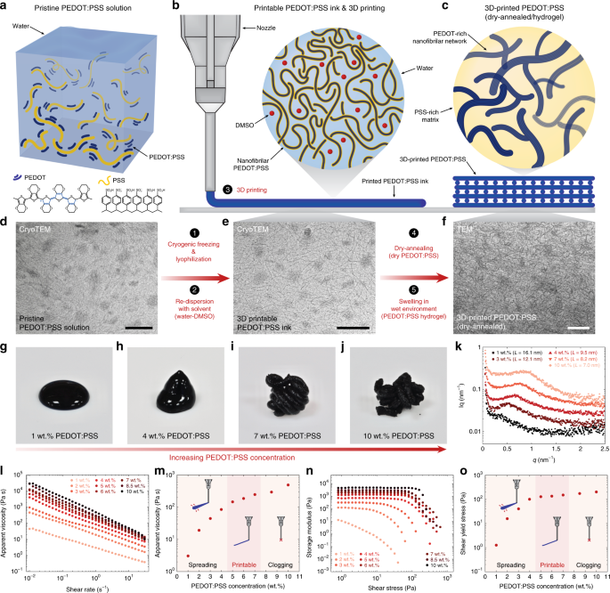
With increasing concentration of the PEDOT:PSS nanofibrils, the suspensions gradually transit from liquids to thixotropic 3D printable inks (Fig. 1g–j) due to the formation of reversible physical networks of the PEDOT:PSS nanofibrils via entanglements within the solvent (Fig. 1e). We perform small angle X-ray scattering (SAXS) and rheological characterizations to quantify microscopic and macroscopic evolutions of the conducting polymer ink with varying concentrations of the PEDOT:PSS nanofibrils, respectively (Fig. 1k–o).
The SAXS characterizations show that the average distance between PEDOT-rich crystalline domains L (d-spacing calculated by the Bragg expression L = 2π/qmax) decreases with an increase in the concentration of the PEDOT:PSS nanofibrils (16.1 nm for 1 wt% and 7.0 nm for 10 wt%), indicating closer packing and higher degree of interactions between the adjacent PEDOT:PSS nanofibrils in more concentrated inks (Fig. 1k).
Rheological measurements of the conducting polymer inks clearly show the transition from low viscosity liquids (low concentration PEDOT:PSS nanofibrils) to physical gels (high concentration PEDOT:PSS nanofibrils) with characteristic shear-thinning and shear-yielding properties for 3D printable inks18,19 (Fig. 1l–o and Supplementary Fig. 2).
The low viscosity and low yield stress of the conducting polymer inks with low PEDOT:PSS nanofibril concentrations (1-4 wt%) cause lateral spreading of 3D-printed inks on the substrate (Fig. 1g, h, m, o). On the other hand, the conducting polymer inks with too high concentrations of PEDOT:PSS nanofibrils (above 8 wt%) start to clog printing nozzles due to the formation of large aggregates of PEDOT:PSS nanofibrils (Fig. 1j, m, o).
Hence, we find that the intermediate range of PEDOT:PSS nanofibril concentrations (5–7 wt%) provides optimal rheological properties and 3D printability (Fig. 1i, m, o). The 3D printable conducting polymer ink can be stored under ambient conditions over a month without the significant change in rheological properties and printability (Supplementary Fig. 3).
After 3D printing, we dry and anneal the 3D-printed conducting polymers to remove solvents (water and DMSO) and facilitate the formation of PEDOT-rich crystalline domains and subsequent percolation among PEDOT:PSS nanofibrils33 (Fig. 1c, f) (see Methods for details). The resultant dry pure PEDOT:PSS can also be readily converted into stable pure PEDOT:PSS hydrogels (equilibrium water contents ~ 87%) by swelling in a wet environment33.
3D printing of conducting polymers
Superior printability of the conducting polymer ink allows various advanced 3D printing capabilities including printing of high resolution, high aspect ratio, and overhanging structures (Fig. 2). To demonstrate high resolution printing in microscale, we print meshes of the conducting polymer ink (7 wt% PEDOT:PSS nanofibril) through 200-, 100-, 50-, and 30-µm diameter nozzles (Fig. 2a–d).
Favorable rheological properties of the conducting polymer ink further enable the fabrication of multi-layered high aspect ratio microstructures (100-µm nozzle, 20 layers) (Supplementary Movie 1) as well as overhanging features (Supplementary Movie 2) (Fig. 2e, h).
The 3D-printed conducting polymer structures can readily be converted into dry and hydrogel forms without loss of the original microscale structures, owing to the constrained drying (while attached on the substrate) and swelling property of the pure PEDOT:PSS hydrogels33 (Fig. 2f, g and Supplementary Fig. 4).
Furthermore, the 3D-printed conducting polymer hydrogels exhibit long-term stability in physiological wet environments without observable degradation of microscale features (e.g., high aspect ratio and overhanging structures) after storing in PBS for 6 months (Supplementary Fig. 5).
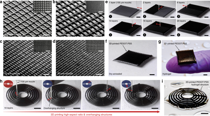
The 3D printable conducting polymer ink can be readily incorporated into multi-material 3D printing processes together with other 3D printable materials. For example, we fabricate a structure that mimics a high-density multi-electrode array (MEA) based on multi-material 3D printing of the conducting polymer ink and an insulating polydimethylsiloxane (PDMS) ink with a total printing time less than 30 min (Supplementary Fig. 6a, b and Supplementary Movie 3).
The 3D-printed MEA-like structure shows a complex microscale electrode pattern and a PDMS well that are comparable to a commercially available MEA fabricated by multi-step lithographic processes and post-assembly (Supplementary Fig. 6c).
Properties of 3D-printed conducting polymers
The 3D-printed conducting polymers can achieve electrical conductivity as high as 155 S cm−1 in the dry state and 28 S cm−1 in the hydrogel state, comparable to the previously reported high-performance conducting polymers5,16,33 (Fig. 3a, Supplementary Fig. 7, and Supplementary Table 2).
Notably, a smaller nozzle diameter yields a higher electrical conductivity for the printed conducting polymers, potentially due to shear-induced enhancements in the PEDOT:PSS nanofibril alignment22.
Flexibility of the 3D-printed conducting polymers allows mechanical bending with maximum strain of 13% in the dry state (65 µm radius of curvature with 17 µm thickness) and 20% in the hydrogel state (200 µm radius of curvature with 78 µm thickness) without failure (Supplementary Fig. 8).
To investigate the effect of mechanical bending on the electrical performance, we characterize the electrical conductivity of the 3D-printed conducting polymers (100-µm nozzle, 1 layer) on flexible polyimide substrates as a function of the bending radius as well as the bending cycle (Fig. 3b, c).
The 3D-printed conducting polymers show small changes in the electrical conductivity (less than 5%) across a wide range of tensile and compressive bending conditions (radius of curvature, ±1–20 mm) in both the dry and hydrogel states (Fig. 3b). Furthermore, the 3D-printed conducting polymers can maintain a high electrical conductivity (over 100 S cm−1 in dry state and over 15 S cm−1 in hydrogel state) after 10,000 cycles of repeated bending (Fig. 3c).
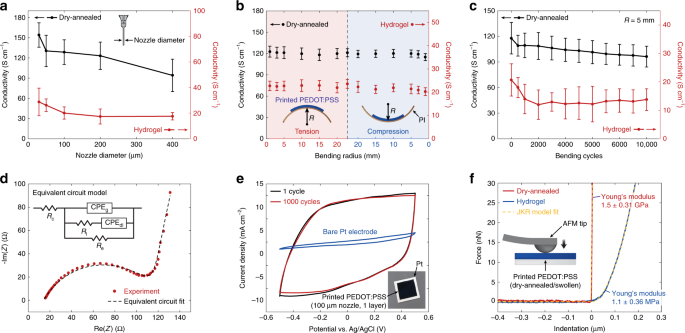
To further investigate the electrical properties, we perform the electrochemical impedance spectroscopy (EIS) of the 3D-printed conducting polymers (100-µm nozzle, 1 layer on Pt) (Fig. 3d).
The EIS data are fitted to the equivalent circuit model shown in Fig. 3d, where Re represents the electronic resistance, Ri represents the ionic resistance, Rc represents the total ohmic resistance of the electrochemical cell assembly, and CPEdl and CPEg represent the constant phase elements (CPE) corresponding to the double-layer ionic capacitance and the geometric capacitance, respectively37,38.
The semicircular Nyquist plot shape suggests the presence of comparable ionic and electronic conductivity in the 3D-printed conducting polymer hydrogels (Fig. 3d), which is confirmed by the extracted fitting parameters of the equivalent circuit model where the ionic and electronic resistances show comparable magnitudes (Ri = 105.5 Ω and Re = 107.1 Ω).
The cyclic voltammetry (CV) demonstrates a high charge storage capability (CSC) of the 3D-printed conducting polymers (100-µm nozzle, 1 layer on Pt) compared to typical metallic electrode materials such as Pt with remarkable electrochemical stability (less than 2% reduction in CSC after 1000 cycles) (Fig. 3e).
The CV of the 3D-printed conducting polymers further shows broad and stable anodic and cathodic peaks under varying potential scan rates39, suggesting non-diffusional redox processes and electrochemical stability of the 3D-printed conducting polymers (Supplementary Fig. 9).
To quantify mechanical properties of the 3D-printed conducting polymers, we conduct nanoindentation tests (Fig. 3f and Supplementary Fig. 10). The 3D-printed conducting polymers display relatively high Young’s modulus of 1.5 ± 0.31 GPa in the dry state, similar to the previously reported values for dry PEDOT:PSS40 (Fig. 3f).
In contrast, the 3D-printed conducting polymers in the hydrogel state exhibit three orders of magnitude reduction in Young’s modulus to 1.1 ± 0.36 MPa, comparable to those of soft elastomers such as PDMS (Young’s modulus, 1–10 MPa) (Fig. 3f). The softness of 3D-printed conducting polymer hydrogels can offer favorable long-term biomechanical interactions with biological tissues, which may find a particular advantage in bioelectronic devices and implants3,41,42.
3D printing of conducting polymer devices
Enabled by the superior 3D printability and properties, 3D printing of the conducting polymer ink can offer a promising route for facile and streamlined fabrication of high resolution and multi-material conducting polymer structures and devices (Fig. 4 and Supplementary Table 1).
Highly reproducible 3D printing of conducting polymers in high resolution allows the rapid fabrication of over 100 circuit patterns with less than 100 µm feature size on a flexible polyethylene terephthalate (PETE) substrate by a single continuous printing process with a total printing time less than 30 min (Fig. 4a, Supplementary Fig. 11, and Supplementary Movie 4).
The resultant 3D-printed conducting polymer electronic circuits exhibit high electrical conductivity to operate electrical components such as a light emitting diode (LED) (Fig. 4b and Supplementary Movie 4) and flexibility to withstand bending without mechanical failure (Fig. 4c).
This programmable, high resolution, and high throughput fabrication of conducting polymer patterns by 3D printing can potentially serve as an alternative to ink-jet printing and screen printing with a higher degree of flexibility in the choice of designs based on applicational demands4,7.
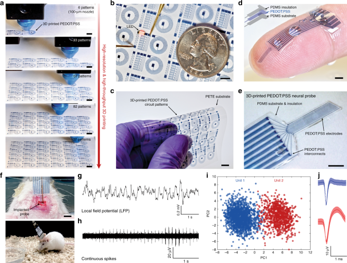
We further demonstrate a facile fabrication of a soft neural probe for in vivo bioelectronic signal recording (Supplementary Fig. 12 and Supplementary Movie 5). The multi-material 3D printing capability in high resolution allows us to print both insulating encapsulation (PDMS ink) and electrodes (conducting polymer ink) of the neural probe by a facile continuous printing process (a total printing time less than 20 min) without the need of post-assemblies or complex multi-step procedures in conventional fabrication methods such as electron-beam lithography15,16 (Fig. 4d, Supplementary Fig. 12, and Supplementary Movie 5).
The resultant probe consists of nine PEDOT:PSS electrode channels in the feature size of 30 µm in diameter with the impedance in the range of 50–150 kΩ at 1 kHz, suitable for in vivo recording of neural activities43,44.
After the connector assembly (Supplementary Fig. 13), the 3D-printed soft neural probe is implanted to the mouse dorsal hippocampus (dHPC, coordinate: −1.8 mm AP; 1.5 mm ML; −1.0 mm DV) with the help of a plastic catheter (Fig. 4f, top). The 3D-printed soft neural probe can successfully record continuous neural activities in a freely moving mouse (Fig. 4f, bottom) from each channel including the local field potential (LFP; at 1 kHz) (Fig. 4g) and the action potential (AP; at 40 kHz) (Fig. 4h) over two weeks. Furthermore, the 3D-printed soft neural probe can record signals from distinctive single units, isolated from individual channel of the probe (Fig. 4i, j).
Source:
MIT


