


 Extract (6-MSITC) in Healthy Older Adults")
: An In-Depth Exploration into its Thermogenic Role and Social Significance")


Many species have naturally evolved remarkable strategies to visually adapt to their environments for protection and predation.
Researchers have studied adaptive camouflaging in the infrared (IR) spectrum, although the method is highly challenging to develop in the lab.
In a new report now published on Science Advances, Mingyang Li and a research team at the National University of Defense Technology in China, developed adaptive thermal camouflage devices that bridged the optical and radiative properties of nanoscopic platinum (Pt) and silver (Ag) electro-deposited Pt films.
The metal-based devices maintained large, uniform, and consistent IR tunabilities in the mid-wave IR (MWIR) and long-wave IR (LWIR) atmospheric transmission windows (ATWs). The team multiplexed and enlarged the devices, allowing flexibility for camouflaging capabilities.
The technology is advantageous across a variety of camouflage platforms and in many thermal radiation management technologies.
Recent years have seen extensive research efforts to control the infrared (IR) features of objects for camouflage in the IR spectrum. To achieve this goal, scientists must precisely control the radiant heat emitted from an object to match the background.
Based on the Stefan-Boltzmann law, the radiant heat of an object is proportional to the fourth power of its absolute temperature and the emittance of the surface. For dynamic control of the temperature or thermal emittance of the object, scientists offer microfluidic networks and thermoelectric systems as possible approaches to maintain adaptive thermal camouflage.
Inspired by the multiple optical and radiative properties of metals, Li et al. reported on nanoscopic platinum (Pt) film-based reversible silver (Ag) electrodeposition (RSE) devices for excellent adaptive thermal camouflage capabilities.
Since nanoscopic platinum films have high IR absorption and partial IR transmission, this could be transformed to absorption via the IR-absorbing gel electrolyte layer in the setup. Applying the deposition voltage in the system allowed gradual electrodeposition of silver on the nanoscopic platinum films, gradually converting the IR absorption and transmission to IR reflection to enable low-emittance states from the devices.
Nanoscopic Pt films could not be dissolved, therefore, they allowed multiple cycles of Ag deposition and dissolution, in order to switch between high and low-emittance states for many cycles. Li et al. developed diverse devices with multiple structural coatings, rough and flexible substrates to form multiplexed formats to expand the camouflaging scenarios.

To explore the regulation of IR on the metal-based devices, the team first studied the electrical properties of the nanoscopic Pt films. They examined the spectral responses of the film, where increasing the Pt thickness showed huge decreases in IR transmittance to indicate that the IR absorption dominated the spectral response of the thin films.
The scientists further examined the potential ranges of IR modulation and the cycling stability of the nanoscopic platinum films in a three-electrode reversible silver electrodeposition (RSE) film.
Due to the energy favorable interface between Ag and Pt, the electrodeposited Ag film showed comparatively more uniform, coherent and fine-grained morphologies on the 3 nm Pt film.
This feature allowed the scientists to convert the nanoscopic Pt film to a high IR reflective film in a short period of time. The nearly identical potentiostatic cycling curves in the system confirmed their ability to perform stable and reversible electrodeposition on the nanoscopic Pt films.
To assess the IR performance of the assembled devices with varying Pt thicknesses, Li et al. attached them on to a 500C hot plate and recorded their real-time MWIR (mid-wave IR) and LWIR (long-wave IR) images.
The team applied a negative voltage of 2.2 V to gradually electrodeposit Ag films on the Pt surface, as the apparent temperature of these devices gradually decreased. When the researchers applied a positive voltage of 0.8 V thereafter, the electrodeposited Ag film could be completely dissolved into the electrolyte, and turned to their initial states to indicate the reversibility of the devices. The device could function steadily for up to 350 fully reversible cycles to confirm their stability and reversibility for adaptive thermal camouflage.

To multiplex and enlarge the device, Li et al. constructed a three-by-three multiplexed IR switchable array and an enlarged independent device. By controlling the combined electrodeposition time of its independent pixels, the scientists generated the letters “N”, “U”, “D”, and “T” with different temperatures as LWIR images on the array.
The work showed the adaptability of the complex background and large-area feasibility of the adaptive systems. The team next expanded the camouflaging scenario of the metal-based dynamic IR modulation mechanism on rough and flexible devices. During the work they replaced polished barium fluoride (BaF2) substrates with rough versions and used polypropylene (PP) films to deposit the nanoscopic Pt films.
Due to the micron-scale roughness of BaF2 and poor wettability of the PP film, the team noted the requirement for thicker Pt films to form physically connected and electrically conductive films.
The rough BaF2-based device diffusely reflected the outside thermal matrix in the setup and suppressed its own IR radiation to effectively reduce the impact from the external environment. The rough and flexible adaptive variants developed in the work highlighted the multi-substrate compatibility of the metal-based IR modulation mechanism, which expanded the camouflaging scenarios of the device.

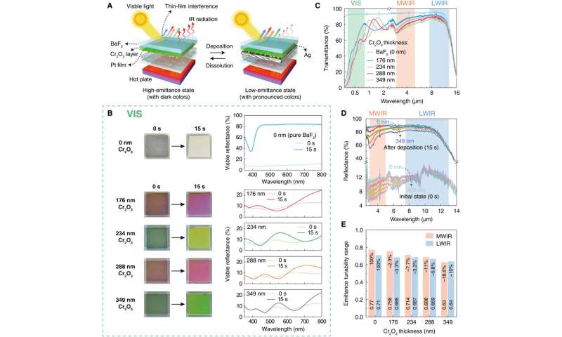
Li et al. then combined the devices with structural color coatings to improve their visible compatibility so as to prevent their visible detection in daytime. For this, they used a series of visible-wavelength-scale, thick chromium oxide (Cr2O3) layers between the BaF2 substrate and nanoscopic Pt films. Upon depositing different thicknesses of Cr2O3 layers, due to their thin-film interference effects in the visible spectrum, the “decorated” devices displayed various colors.
The scientists noted the structural colors to shift from relatively dark to more pronounced colors in the setup. The Cr2O3 layers only generated colors in the visible spectrum and therefore exerted little influence on the IR performance of the devices. The results showed the possibility of integrating simple optical designs into the adaptive systems for visible compatibility, making the devices more difficult to detect in the daytime.
In this way, Mingyang Li and colleagues developed adaptive camouflage devices by reversibly depositing silver on nanoscopic platinum films. The devices showed large, uniform, and consistent IR tunabilities in both mid-wave IR and longwave IR atmospheric transmission windows.
The scientists easily multiplexed the devices by patterning nanoscopic Pt films or by adding conductive grids for complex background adaptability and large-area flexibility. The team achieved visible compatibility by adding a series of visible-wavelength-scale-thick Cr2O3 layers.
The devices developed in this work can inspire the next generation of adaptive thermal camouflage platforms that rapidly and precisely control thermal radiation and camouflage in response to multispectral detection and adaptability to complex environments. These devices will have applications across thermal radiation management techniques including energy efficient buildings, thermoregulation clothes and in smart spacecrafts.
Graphene Based Adaptive Thermal Camouflage
The ability to control thermal radiation from a hot object has both scientific1-5 and technological importance2, 6-8.The radiated thermal energy per unit area from a hot surface is characterized by the Stefan–Boltzmann law, P = εσT4 where ε is the emissivity of the surface, σ is the Stefan–Boltzmann constant and T is the temperature of the surface.
The emissivity is the only material-dependent parameter that varies with the wavelength and temperature.
At thermodynamic equilibrium, Kirchhoff’s radiation law connects the wavelength-specific thermal emissivity with the optical absorption of the surface as ε (T ,λ) = α(T , λ ) .
One can engineer the thermal radiation by coating the surface with photonic crystals5, 9-11 or plasmonic structures12.
The dynamic control of thermal radiation, however, requires ability to alter optical absorption via electrical means. Phase change materials13-16, quantum wells17, electrochromic dyes18, ferroelectric materials19 or plasmonic resonators12, 20, 21 have all been investigated for tunable infrared emission.
These research efforts on dynamic control of thermal radiation have encountered various problems such as, low tunability19, 20, 22, narrow spectral window17, slow response speed18 and rigid substrates17.
Electrochromic materials have been the most promising one23-25, however, the requirement of a top metallic contact layer and volatile electrolytes limit their performance (see the benchmarking in Table S1). These challenges have been hindering the realization of adaptive thermal camouflage systems.
Graphene provides new perspectives to control electromagnetic radiation in a very broad spectral range, from visible to microwave frequencies26-28. Optical absorption of graphene can be tuned by electrostatic gating owing to the Pauli blocking29,30.
Although, optical response of graphene has been studied extensively, the use of graphene for dynamic control of thermal radiation has remained unexplored because of the small optical absorption (< 2%) in mid-IR region31.
In this work, we developed a new class of active thermal surfaces using multilayer graphene which yields significant tunable optical absorption in IR region. Since thermal radiation originates from the very top surface, top-gating or electrolyte gating schemes are not suitable for the control of thermal radiation.
These gating methods generate either buried graphene surfaces or low electrostatic doping29,32, which yields negligible IR modulation. None of the previously reported graphene devices by our group and others is suitable for dynamic control of thermal radiation.
Therefore, we introduce a new gating scheme using an inverse device structure which leads intercalation of a nonvolatile ionic liquid into graphene layers from the porous substrate.
This inverse device configuration yields an uncovered graphene surface with tunable charge density and Fermi energy. Figure 1a shows the schematic of the active thermal surface consisting of a multilayer-graphene electrode on a porous polyethylene (PE) membrane and a back gold-electrode.
We synthesized multilayer-graphene on nickel foils using a chemical vapor deposition method and then transferred them on PE membrane which is IR transparent and can hold the electrolyte (room-temperature ionic liquid, RTIL).
The thermal radiation emitted by the device mainly originate from the top graphene electrode since the emissivity of gold-coated substrate is very low (<0.01) due to its highly reflective nature, and the PE membrane is IR transparent.
Figure 1b illustrates the working principle of the active thermal surface. Under a voltage bias, the ionic liquid intercalates into the graphene layers, and dopes them. As a result of doping, the charge density on graphene increases and Fermi-level shifts to higher energies, which suppresses the IR absorption and thus the emissivity of the graphene electrode30.
Figure 1c and 1d show the thermal camera images of the fabricated device at 0 and 3V, respectively. At 0 V, the temperature profile of the background (author’s hand) can be seen through the device. However, at 3 V, the emissivity of the device is significantly suppressed, which screens the background temperature profile (Movie S1).
The emissivity of the device can be switched between high and low states many times with response time< 1s. These devices are thin, light, and flexible that can easily cover their environment (Figs. S1 and S2).

To quantify the performance of the fabricated active thermal surfaces, we first placed them on a hot plate at 55 °C and recorded the thermal images (Figure 2a, 2b and Figure S1 and Movie 2), at different bias voltages between 0 and 4 V. Note that, the voltage range is limited by the electrochemical window of the room temperature ionic liquid33.
We obtained the best performance with the IL [DEME][TFSI] which yields relatively large electrochemical window up to 4 V. The thermograms show substantial change in the thermal appearance which is quite homogenous over a large area device (10×9 cm2).
The IR camera renders the thermograms assuming a constant emissivity of 1. Although the temperature of the device is the same, the gold electrode appears cold at high voltages due to its low emissivity.
First, we measured the IR spectrum of the emitted radiation at different bias voltages (Figure 2c) using a Fourier transform infrared spectrometer (FTIR). The modulation of spectral radiance of the device covers the full mid-infrared range.
The intensity of the spectrum decreases by a factor of 2.5 at 3.5 V over a broad range. To measure the variation of the total emitted thermal power from the device, we used a thermopile sensor which performs a differential measurement with respect to the room temperature (inset in Figure 2d).
We recorded the output voltage of the sensor as we scanned the bias voltage between 0 and 4 V with a scan rate of 0.01 V/s (Supplementary Movie 2). To block the background radiation, we used a 3-inch-silicon- wafer coated with 100 nm thick gold film which has very low emissivity (<0.1). The voltage dependence of emitted power from the device is shown in Figure 2d. We observed a clear step- like behavior with a threshold voltage of 2 V. The emitted thermal power is reduced by a factor of 2.5 at a bias voltage of 3.5 V. These numbers agree very well with the spectral measurements.
To calculate the emissivity of device, we used a carbon nanotube forest as a reference black surface which has emissivity close to 1 (Figure S3)34. The extracted emissivity of the multilayer graphene at 10 µm is reduced from 0.76 down to 0.33 as we scanned the voltage from 0 to 3.5 V (Scattered plot in Figure 2d).
Variation of the total radiated power and the extracted emissivity values show similar voltage dependence indicating that the variation of emissivity with the bias voltage is nearly constant over the mid-IR range. The intercalation process is reversible and the device can be switched between high and low emissivity values with a time constant of 0.5 s.
Our results suggest that, the observed suppression of the emissivity is due to the suppression of IR absorption of multilayer graphene via intercalation of ionic liquid. To further quantify the intercalation process, we measured variation of the sheet resistance of ML-graphene using four-point resistivity method (inset in Figure 2e).
Similarly, the sheet resistance of the graphene electrode shows a step like variation from 33Ω down to 0.6 Ω (Figure 2e). The sheet resistance and the emissivity of ML-graphene are correlated. As the layer number increases both sheet resistance and emissivity decrease (Figure S4).
To gain more insight about the mechanism behind the electrical control of thermal radiation, we performed in situ optical characterization of the ML-graphene electrodes (Figures S5 and S6). We observed that the transmittance of ML- graphene decreased substantially whereas the reflectivity increased due to the high level of doping.
We also tested similar devices with single-layer graphene and observed slight modulation (<2% increase) of thermal radiation due to enhanced inter-band absorption (Figure S7). These results and our electromagnetic simulations reveal that, both inter-band and intra- band transitions of the ML-graphene contribute to the observed emissivity modulation in the IR
spectrum30, 35, 36 (Figure S8). The tunable high mobility free carriers on graphene layers are responsible for the control of the emissivity37, 38.

Using the nonvolatile RTIL electrolyte allows us to operate these devices also in ultrahigh vacuum conditions. This ability is critical for some applications such as active thermal shields for outer space applications23, as well as utilization of surface characterization tools such as X-ray photoelectron spectroscopy (XPS), which can elucidate the operation of the devices in a chemically specific fashion. Although, intercalation of graphitic materials with metallic ions have been studied extensively35, intercalation of ionic liquids remains relatively unexplored33.
Our device lay-out (Figure 3a) provides a unique advantage to characterize the intercalation process. The ionic liquid contains two nitrogen atoms (Figure 3b); one with a positive (quaternized nitrogen) and the other with a negative (imide nitrogen) charge that yield well resolved two N1s peaks.
Figure 3c shows the recorded C1s, N1s and F1s region of XP spectra at different bias voltages. These spectral evolutions provide a wealth of information about the operation of the device.
The appearance of N1s and F1s peaks after 1.5V indicates the onset of the intercalation process and the threshold voltage. Since XPS probes the very top surface (~10 nm) appearance of F1s and N1s peaks shows that the ions can efficiently intercalate the thick active surface (>100 graphene layers).
The intensity of C1s decreases with increasing voltage due to the partial coverage of the top surface with the IL. The C1s peak of the-CF3group associated with IL also appears after the threshold voltage. Although, the graphene surface is grounded, the binding energy of C1s also experiences a small shift with the applied bias, from 284.37 to 283.67 (Figure 3e) most likely due to the shift in the Fermi energy of graphene39.
Interestingly, we observed co-intercalation of anions and cations of the ionic liquid with a significant charge imbalance> 20% (the ratio of N– to N+). This charge imbalance (due to mobile and quasi-independent ions) is responsible for electrostatic doping on graphene layers. When we apply negative bias voltage, the charge imbalance is reversed (Figure 3d).
Our results shows that intercalation of ionic liquid into multilayer graphene yields effectively a charge imbalance with a charge excess of about 1 ion for ~200 C atoms of the intercalated active layer (Figure S9). This direct observation of the chemical contents of intercalate with related electronic properties of the graphene layers will further guide us to optimize the device operation.

recorded in ultra-high vacuum 10-8torr. (d) Variation of the normalized intensities and binding energy of C1s, N1s, and F1s. (e) The variation of the binding energy of C1s and F1s. (f) XPS spectra of N1s showing the charge imbalance for positive and negative bias voltages.
To show one promising application of the developed thermal surfaces, we now would like to demonstrate a functional adaptive camouflage system. In nature, animals developed adaptive camouflage techniques using specialized cells that enable active feedback mechanisms to adjust the skin color and texture1, 40.
Our strategy uses thermal emission as a feedback. Figure 4a shows the working principle of the adaptive thermal camouflage system. The body temperature of the device is set to 40 °C. The thermocouple measures the actual surface temperature and sends the sensory information to the circuit which uses the thermal radiation from the device as a feedback and yield a control signal to adjust the thermal radiation.
The algorithm minimizes the difference between the surface temperature and the apparent temperature of the device. Although the body temperature of the device is constant, by tuning the emissivity of the surface with the control voltage, this device can blend itself with the time varying thermal background.
Figure 4b shows the varying surface temperature (red curve) and apparent temperature of the device (blue curve). After the optimization of the feedback gain, the apparent temperature follows the surface temperature with a small time delay of< 5 s (Figure S10).
When we set a large gain in the control circuit, we observe large oscillations in the apparent temperature, but eventually, the apparent temperate reaches that of the background (Figure S11). This device can operate in the temperature range between 38 and 25 °C.
The dynamic range of the camouflage system depends on many factors; such as the body temperature of the device, modulation of the emissivity, the surface temperature, the background temperature (from the environment) and quality of thermal contact between the object and the active surface.
To obtain the more insight for the operation range and further quantify the experimental observations, we developed a model for the apparent temperature. The thermal camera renders the temperature of a surface from the detected radiation which includes radiation from the surface and the reflected background (environment) radiation as

where Ta, T0 and Tb represent apparent, body and background temperatures, respectively and ε0 is the emissivity of the surface and εc is the emissivity used by the camera. We can write reflectivity of the surface as R = 1 – A = 1 – ε0 where A is the absorption of the surface. (Note thatthe transmission of the device is 0 due to the gold electrode.)
The solid lines in Figure 4c shows the relation between apparent temperature and the actual body temperature for different emissivity range from 0 to 1. For this calculation, we used background temperature of 26.7 °C. We first verify these calculations using a gold-coated surface (εAu~0) and carbon-nanotube sample (εCNT~1).
Gold-coated surface always shows the background temperature due to the perfect IR reflectivity however, CNT sample shows the actual body temperature due to perfect emissivity (no reflectivity, see Figure S12).
Apparent temperature of our device varies between these values depending on the emissivity (ε~ 0.3-0.8) and body temperature. Figure 4c reveals three intriguing results due to the interplay between the radiation and reflection.
First, the dynamic range of the active surface increases with the temperature difference between the body and the background. Second, when the body temperature is the same with background, the apparent temperature of the device does not change with the voltage. The suppression of the emissivity is compensated by the increasing reflectivity.
Third, when the body temperature is lower than the background, the apparent temperature increases with decreasing emissivity (increasing voltage). When the voltage was applied, the cold surface looks hotter. Therefore, the voltage controlled emissivity and reflectivity of ML-graphene enables us to design new camouflage systems that can disguise hot surfaces as cold and cold ones as hot in a thermal imaging system.
When the surface is hotter than the background temperature, the thermal emission is dominant. Suppression of the emissivity of the surface yields colder appearance. However, when the object is colder than the background temperature, the reflection of the background radiation is dominant.
Increasing concentration of high mobility carrier on the graphene surface under a bias voltage yields a hotter appearance in thermal imaging systems.
The thickness of the multilayer graphene is another important parameter that defines the modulation range of the emissivity. We fabricated and characterized a series of devices with varying the thickness of the active graphene layer.
Figure 4d shows the variation of the measured and calculated emissivity with the layer number. The maximum emissivity of 0.8 can be obtained with 100 layers of graphene. Thicker or thinner films yield less emissivity due to larger reflectivity or smaller absorption, respectively.
In Figure 4d, we also show the measured emissivity for the doped graphene (at 3.5V, blue dots). We observed that minimum emissivity also varies with the layer number which is likely due to inefficient intercalation for thick films and residual infrared absorption of doped graphene in Pauli blocking regime which is not fully understood yet. The maximum emissivity modulation can be obtained with 150 layers of graphene.

Finally, we would like to demonstrate an integration scheme which yields more complex reconfigurable thermal images. Figure 5a shows the multipixel device consisting of large area continuous graphene film on PE substrate and 5×5 arrays of individually addressable gold electrodes deposited on a printed circuit board. In this layout, the graphene film is wired to the ground electrode. By controlling voltage of a pixel with an external circuit, we were able to confine the intercalation within the pixel thus results modulation of local emissivity. Figure 5b shows three thermal images of the device with different voltage configurations. For low and high emissivity, we applied -3.5 and 0 V to the pixels, respectively. A temperature contrast of 10 °C can be obtained at each pixel individually (Figure 5c) and can be switched in 0.1 sec (Figure 5d). The crosstalk between the pixels is negligible. With this area selective intercalation, we generated complex thermal images such as a text “HELLO” (See Movie 5). The size of the pixels can be scaled down to millimeter without a significant crosstalk.
These devices can also be fabricated by pattering the graphene layer and using different addressing mechanisms (see Figures S13 and S14). These results show that, our approach can be used to disguise the shape and temperature of objects in thermal imaging systems. Furthermore these devices can also operate as adaptive IR-mirrors.

In conclusion, we have developed a new class of active thermal surfaces capable of efficient real-time electrical-control of their thermal emission over the full infrared spectrum. We showed that emissivity of multilayer graphene electrodes can be controlled electrically between 0.8 down to 0.3 with a bias voltage less than 4 V.
Using these active surfaces, we have demonstrated adaptive camouflage systems that can disguise hot surfaces as cold and cold ones as hot in a thermal imaging system.
Simplicity of the layered device structure together with the efficient modulation over broad IR spectrum (from 2 to 25 µm) provides an unprecedented ability for adaptive thermal camouflage.
These active surfaces are flexible which enable their integration with nonplanar surfaces, such as soft robotic systems2.
Furthermore, these devices can operate at high temperatures and under high vacuum conditions due to low vapor pressure of the ionic liquids enabling us to monitor the intercalation process using X-ray photoelectron spectroscopy.
Our results provide a significant step for realization of adaptive thermal management, which could enable new technologies, not only for thermal camouflage but also for adaptive IR optics and adaptive heat shields for satellites23.
References:
- Ramachandran, V. S.; Tyler, C. W.; Gregory, R. L.; RogersRamachandran, D.; Duensing, S.; Pillsbury, C.; Ramachandran, C. Nature 1996, 379, (6568), 815-818.
- Morin, S. A.; Shepherd, R. F.; Kwok, S. W.; Stokes, A. A.; Nemiroski, A.; Whitesides, G. M. Science 2012, 337, (6096), 828-832.
- Schittny, R.; Kadic, M.; Guenneau, S.; Wegener, M. Physical Review Letters 2013, 110, (19).
- Han, T. C.; Bai, X.; Gao, D. L.; Thong, J. T. L.; Li, B. W.; Qiu, C. W. Physical Review Letters 2014,112, (5).
- Han, T. C.; Bai, X.; Thong, J. T. L.; Li, B. W.; Qiu, C. W. Adv Mater 2014, 26, (11), 1731-1734.
- Yu, C. J.; Li, Y. H.; Zhang, X.; Huang, X.; Malyarchuk, V.; Wang, S. D.; Shi, Y.; Gao, L.; Su, Y. W.; Zhang, Y. H.; Xu, H. X.; Hanlon, R. T.; Huang, Y. G.; Rogers, J. A. Proceedings of the National Academy of Sciences of the United States of America 2014, 111, (36), 12998-13003.
- Raman, A. P.; Anoma, M. A.; Zhu, L.; Rephaeli, E.; Fan, S. Nature 2014, 515, (7528), 540-4.
- Lampert, C. M. Sol Energ Mater 1984, 11, (1-2), 1-27.
- Luo, C. Y.; Narayanaswamy, A.; Chen, G.; Joannopoulos, J. D. Physical Review Letters 2004, 93, (21).
- Laroche, M.; Carminati, R.; Greffet, J. J. Physical Review Letters 2006, 96, (12).
- Han, S. E.; Norris, D. J. Phys Rev Lett 2010, 104, (4), 043901.
- Tsai, M. W.; Chuang, T. H.; Meng, C. Y.; Chang, Y. T.; Lee, S. C. Applied Physics Letters 2006, 89, (17).
- Kats, M. A.; Blanchard, R.; Zhang, S. Y.; Genevet, P.; Ko, C. H.; Ramanathan, S.; Capasso, F. Phys Rev X 2013, 3, (4).
- Bessiere, A.; Marcel, C.; Morcrette, M.; Tarascon, J. M.; Lucas, V.; Viana, B.; Baffier, N. J Appl Phys 2002, 91, (3), 1589-1594.
- Sauvet, K.; Sauques, L.; Rougier, A. Sol Energ Mat Sol C 2009, 93, (12), 2045-2049.
- Xiao, L.; Ma, H.; Liu, J. K.; Zhao, W.; Jia, Y.; Zhao, Q.; Liu, K.; Wu, Y.; Wei, Y.; Fan, S. S.; Jiang, K. L.Nano Letters 2015, 15, (12), 8365-8370.
- Inoue, T.; De Zoysa, M.; Asano, T.; Noda, S. Nat Mater 2014, 13, (10), 928-31.
- Hutchins, M. G.; Butt, N. S.; Topping, A. J.; Gallego, J.; Milne, P.; Jeffrey, D.; Brotherston, I.Electrochim Acta 2001, 46, (13-14), 1983-1988.
- Huang, Y.; Boriskina, S. V.; Chen, G. Applied Physics Letters 2014, 105, (24).
- Vassant, S.; Doyen, I. M.; Marquier, F.; Pardo, F.; Gennser, U.; Cavanna, A.; Pelouard, J. L.; Greffet, J. J. Applied Physics Letters 2013, 102, (8).
- Schuller, J. A.; Taubner, T.; Brongersma, M. L. Nature Photonics 2009, 3, (11), 658-661.
- Jun, Y. C.; Luk, T. S.; Ellis, A. R.; Klem, J. F.; Brener, I. Applied Physics Letters 2014, 105, (13).
- Demiryont, H.; Moorehead, D. Sol Energ Mat Sol C 2009, 93, (12), 2075-2078.
- Li, H.; Xie, K.; Pan, Y.; Yao, M.; Xin, C. Synthetic Met 2009, 159, (13), 1386-1388.
- Mortimer, R. J. Annu Rev Mater Res 2011, 41, 241-268.
- Sensale-Rodriguez, B.; Yan, R.; Kelly, M. M.; Fang, T.; Tahy, K.; Hwang, W. S.; Jena, D.; Liu, L.; Xing, H. G. Nature communications 2012, 3, 780-786.
- Zhang, X.; Liu, M.; Yin, X. B.; Ulin-Avila, E.; Geng, B. S.; Zentgraf, T.; Ju, L.; Wang, F. Nature 2011,474, (7349), 64-67.
- Balci, O.; Polat, E. O.; Kakenov, N.; Kocabas, C. Nature communications 2015, 6.
- Polat, E. O.; Kocabas, C. Nano Letters 2013, 13, (12), 5851-5857.
- Bao, W. Z.; Wan, J. Y.; Han, X. G.; Cai, X. H.; Zhu, H. L.; Kim, D. H.; Ma, D. K.; Xu, Y. L.; Munday, J. N.; Drew, H. D.; Fuhrer, M. S.; Hu, L. B. Nature communications 2014, 5.
- Brar, V. W.; Sherrott, M. C.; Jang, M. S.; Kim, S.; Kim, L.; Choi, M.; Sweatlock, L. A.; Atwater, H. A.Nature communications 2015, 6, 7032.
- Polat, E. O.; Balci, O.; Kocabas, C. Sci Rep-Uk 2014, 4.
- Armand, M.; Endres, F.; MacFarlane, D. R.; Ohno, H.; Scrosati, B. Nature Materials 2009, 8, (8), 621-629.
- Mizuno, K.; Ishii, J.; Kishida, H.; Hayamizu, Y.; Yasuda, S.; Futaba, D. N.; Yumura, M.; Hata, K. Proceedings of the National Academy of Sciences of the United States of America 2009, 106, (15), 6044- 6047.
- Dresselhaus, M.; Dresselhaus, G. Adv Phys 1981, 30, (2), 139-326.
- Hennig, G. The Journal of chemical physics 1965, 43, (4), 1201-1206.
- Solanki, A. K.; Kashyap, A.; Nautiyal, T.; Auluck, S.; Khan, M. A. Solid State Commun 1996, 100, (9), 645-649.
- Taft, E. A., and H. R. Philipp. . Physical Review . 1965, 138, (1A ), A197.
- Copuroglu, M.; Aydogan, P.; Polat, E. O.; Kocabas, C.; Suzer, S. Nano Letters 2014, 14, (5), 2837- 2842.
- Kreit, E.; Mathger, L. M.; Hanlon, R. T.; Dennis, P. B.; Naik, R. R.; Forsythe, E.; Heikenfeld, J. J R Soc Interface 2013, 10, (78).
More information: Mingyang Li et al. Manipulating metals for adaptive thermal camouflage, Science Advances (2020). DOI: 10.1126/sciadv.aba3494
Chengyi Xu et al. Adaptive infrared-reflecting systems inspired by cephalopods, Science (2018). DOI: 10.1126/science.aar5191
Rinu Abraham Maniyara et al. Tunable plasmons in ultrathin metal films, Nature Photonics (2019). DOI: 10.1038/s41566-019-0366-x


