


 Extract (6-MSITC) in Healthy Older Adults")
: An In-Depth Exploration into its Thermogenic Role and Social Significance")


By integrating a light-emitting electrochemical cell with a resistive random-access memory that are both based on perovskite, the team achieved parallel and synchronous reading of data both electrically and optically in a ‘light-emitting memory.’
At the most fundamental level, digital data is stored as a basic unit of information known as a bit, which is often represented as either a one or a zero. Thus, the pursuit of better data storage comes down to finding more efficient ways to store and read these ones and zeros.
One candidate is nonvolatile resistive random-access memory, or RRAM. Instead of storing charge in transistors like in flash memory, resistive memory uses materials that can switch between states of high and low resistance to represent ones and zeros.
“However, the electrical measurements needed to check the resistance and read zeros and ones from RRAM can limit the overall speed,” explains Chun-Chieh Chang, professor at National Taiwan Normal University and one of the corresponding authors of the study published in Nature Communications.
“Recently, to overcome this issue, RRAMs have been combined with LEDs to develop something called light-emitting memories. In this case, the data can also be read by checking if the LED is on or off. This additional optical reading also opens new routes for carrying large amounts of information.”
To overcome this, the researchers turned to perovskite, a type of material with a crystalline structure through which ions can migrate to give it unique physical, optical, and even electrical properties. By controlling the ion migration, perovskite researchers have been constructing new materials with unique properties.
“Using just one perovskite layer between contacts, we could fabricate a device that works both as a RRAM and a light-emitting electrochemical cell,” explains National Taiwan Normal University’s Ya-Ju Lee, who also led the study.
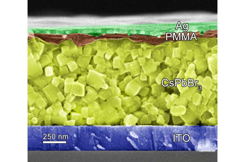
Using perovskite consisting of cesium lead bromide (CsPbBr3), the team demonstrated that data can be electrically written, erased, and read in one of the perovskite devices acting as an RRAM. Simultaneously, the second perovskite device can optically transmit whether data is being written or erased through light emission by working as a light-emitting electrochemical cell with a high transmission speed.
Furthermore, the researchers used perovskite quantum dots of two different sizes for the two devices in the light-emitting memory to achieve different emission colors depending on whether the memory was being written or erased, providing a real-time indicator of the ones and zeros.
Kaoru Tamada, a distinguished professor at Kyushu University’s Institute for Materials Chemistry and Engineering who was also involved in the project, sees many opportunities for this new technology going forward.
“This demonstration significantly broadens the scope of applications of the developed all-perovskite light-emitting memory and can serve as a new paradigm of synergistic combination between electronic and photonic degrees of freedom in perovskite materials,” says Tamada.
“From multicast mesh network to data encryption systems, these findings have the potential for numerous applications in next-generation technologies.”
Discussion
In conclusion, a fast, all-perovskite-based LEM is demonstrated for the first time by employing the outstanding electrical and optical properties of the CsPbBr3 QDs in a simple Ag/PMMA/CsPbBr3 QDs/ITO structure. The electrically driven ionic motions in the perovskite QD layer enable this structure to function either as a fast, reliable electrical memory, or a fast, efficient light source, and more importantly, the swift switching between the dual functionalities of the same structure by simply modulating its bias polarity.
The highly-efficient optical transitions in the perovskite QD layer accompanied by the tunable emission colors not only allow for the realization of the LEM in the same material system through monolithic integration, but also the enhanced functionalities of the LEM to broaden the scope of its applications. We believe that this work could lead to more powerful perovskite-based devices based on a more complicated device architecture, featuring high integration density, fast modulation speed, and multiple device functionality.
reference link : More information: Meng-Cheng Yen et al, All-inorganic perovskite quantum dot light-emitting memories, Nature Communications (2021). DOI: 10.1038/s41467-021-24762-w


